Advertisement
Grab your lab coat. Let's get started
Welcome!
Welcome!
Create an account below to get 6 C&EN articles per month, receive newsletters and more - all free.
It seems this is your first time logging in online. Please enter the following information to continue.
As an ACS member you automatically get access to this site. All we need is few more details to create your reading experience.
Not you? Sign in with a different account.
Not you? Sign in with a different account.
ERROR 1
ERROR 1
ERROR 2
ERROR 2
ERROR 2
ERROR 2
ERROR 2
Password and Confirm password must match.
If you have an ACS member number, please enter it here so we can link this account to your membership. (optional)
ERROR 2
ACS values your privacy. By submitting your information, you are gaining access to C&EN and subscribing to our weekly newsletter. We use the information you provide to make your reading experience better, and we will never sell your data to third party members.
Physical Chemistry
Quantum Control Of Diamond Structures
Quantum effects may govern the formation of nanostructures on the surface of boron-doped diamond microcrystals
by Jyllian N. Kemsley
April 13, 2009
| A version of this story appeared in
Volume 87, Issue 15

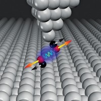
Quantum effects may govern the formation of nanostructures on the surface of boron-doped diamond microcrystals, reports a group led by Igor B. Altfeder of the Air Force Research Laboratory and Jacqueline Krim of North Carolina State University (Phys. Rev. Lett. 2009, 102, 136104). Quantum control of structures, thought to be governed by the wavelengths of electrons, has previously been observed in molecular assembly on a copper surface and in thin metal films. In the new study, the researchers used scanning tunneling microscopy (STM) to investigate the surface structures of pure and boron-doped diamond microcrystals. On the boron-doped crystals they found parallelogram-shaped grains that were 10.5 nm long, 8.3 nm wide, and at least 1.5 nm tall. Because the features are not observed on pure diamond, the scientists postulate that the boron dopant, which gives diamond metallic properties, induces quantum effects that control the growth of the nanostructures. Within the parallelograms are features spaced 3.5 nm apart. The features are due to lateral standing electron waves, the likely driving force of the electronic growth mechanism, the researchers say.


Join the conversation
Contact the reporter
Submit a Letter to the Editor for publication
Engage with us on Twitter