Advertisement
Grab your lab coat. Let's get started
Welcome!
Welcome!
Create an account below to get 6 C&EN articles per month, receive newsletters and more - all free.
It seems this is your first time logging in online. Please enter the following information to continue.
As an ACS member you automatically get access to this site. All we need is few more details to create your reading experience.
Not you? Sign in with a different account.
Not you? Sign in with a different account.
ERROR 1
ERROR 1
ERROR 2
ERROR 2
ERROR 2
ERROR 2
ERROR 2
Password and Confirm password must match.
If you have an ACS member number, please enter it here so we can link this account to your membership. (optional)
ERROR 2
ACS values your privacy. By submitting your information, you are gaining access to C&EN and subscribing to our weekly newsletter. We use the information you provide to make your reading experience better, and we will never sell your data to third party members.
Materials
Big Graphene
New methods yield industrial-sized sheets of ultrathin carbon
by Mitch Jacoby
July 5, 2010
| A version of this story appeared in
Volume 88, Issue 27
In the couple of years since graphene stormed onto the materials research scene and became the popular new kid on the block, this ultrathin carbon material’s rock-star status has moved in just one direction: up. The word on the street is that graphene may have the potential to step in as silicon’s successor for some electronics applications. To realize that potential, however, scientists need to devise ways to prepare high-quality graphene sheets in large size and bulk quantity. A few research teams report doing just that.
Graphene’s outstanding electrical, mechanical, and chemical properties make it a top choice for displays and other flexible electronics applications, says Byung Hee Hong, a chemistry professor at Sungkyunkwan University (SKKU), in Suwon, South Korea. But efforts to make transparent conducting films from graphene have been hampered by the inability to synthesize, transfer, and dope graphene at the scale and quality required for commercial applications, he says.
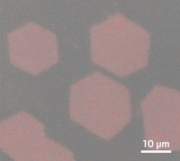
Last year, Hong’s group reported a strategy for making centimeter-sized patterned graphene films via a chemical vapor deposition method. That work marked a significant advance compared with the earliest methods of isolating microscopic single-layer graphene flakes by peeling apart graphite layers with the aid of adhesive tape (C&EN, March 2, 2009, page 14).
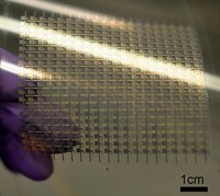
Just recently, Hong’s team demonstrated an industrial-style roll-to-roll process for making rectangular graphene films measuring 30 inches along the diagonal (Nat. Nanotech., DOI: 10.1038/nnano.2010.132). The films exhibit lower sheet resistance and higher optical transmittance than commercial transparent electrodes, such as ones made from indium tin oxide (ITO), the team reports. The research group, which also includes SKKU materials scientist Jong-Hyun Ahn and coworkers in Singapore and Japan, used the films to fabricate flexible electrodes and incorporated them into the first fully functioning graphene-based touch-screen panel device.
The researchers grew the films on a copper foil roll via chemical vapor deposition from a methane-hydrogen mixture. Then they used a system of rollers to attach the film to a thermal-release tape, etched away the foil, and transferred the film (in this demonstration) to a polyethylene terephthalate substrate. Then they printed electrodes and other circuit elements onto the transparent conducting graphene/PET film.

Other graphene preparation methods are also delivering big results. For example, at Rensselaer Polytechnic Institute, a team led by physics professor Swastik Kar devised a scalable, mild procedure using 1-pyrenecarboxylic acid to readily wedge apart graphite into aqueous dispersions of single- and few-layer graphene flakes (Nano Lett., DOI: 10.1021/nl903557p).
And at the Leibniz Institute for Solid State & Materials Research, in Dresden, Germany, Victor Yu. Aristov and coworkers demonstrated that large graphene films can be synthesized by thermal decomposition of commercially available β-SiC substrates measuring more than 300 mm in diameter (Nano Lett., DOI: 10.1021/nl904115h).
“The rapidly rising cost of ITO is a serious problem,” says Samsung Electronics principal engineer Yoonho Khang, who is located in South Korea. These new methods for making a low-cost replacement material such as graphene may have “a huge impact on the display industry.”
Columbia University physics professor Philip Kim is amazed at the pace of recent progress. “Graphene is really getting close to commercial applications,” he says. Just a year or two ago, researchers were debating strategies to overcome the challenge of making large samples. “At least in that regard,” Kim says, “we are now exceeding our expectations by far more than we could have imagined.


Join the conversation
Contact the reporter
Submit a Letter to the Editor for publication
Engage with us on Twitter