Advertisement
Grab your lab coat. Let's get started
Welcome!
Welcome!
Create an account below to get 6 C&EN articles per month, receive newsletters and more - all free.
It seems this is your first time logging in online. Please enter the following information to continue.
As an ACS member you automatically get access to this site. All we need is few more details to create your reading experience.
Not you? Sign in with a different account.
Not you? Sign in with a different account.
ERROR 1
ERROR 1
ERROR 2
ERROR 2
ERROR 2
ERROR 2
ERROR 2
Password and Confirm password must match.
If you have an ACS member number, please enter it here so we can link this account to your membership. (optional)
ERROR 2
ACS values your privacy. By submitting your information, you are gaining access to C&EN and subscribing to our weekly newsletter. We use the information you provide to make your reading experience better, and we will never sell your data to third party members.
Materials
Patterned Polymer Nanowire Arrays
Polymer nanowires can be fabricated on a large scale via a combination of laser patterning and plasma etching
by Mitch Jacoby
January 10, 2011
| A version of this story appeared in
Volume 89, Issue 2
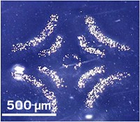
Arrays of polymer nanowires can be fabricated on a large scale from various types of polymers by using a process that combines laser interference patterning and inductively coupled plasma etching, according to a U.S.-Chinese research team (ACS Nano, DOI: 10.1021/nn103319p). Numerous methods are available for preparing arrays of semiconductor and other types of inorganic nanowires. But few techniques have been demonstrated for making organic or polymeric nanowires, and even fewer methods have been developed for preparing these materials as patterned arrays. Developing new ways of making such arrays could lead to advances in the fields of organic light-emitting diodes and solar cells. Zhong Lin Wang and Hao Fang of Georgia Institute of Technology and coworkers there and at Peking University exposed polymer films to interference patterns formed by crossing a pair of laser beams. The process, which was applied separately to UV-absorbent and non-UV-absorbent films, generated ablation trenches with patterns and dimensions that could be controlled by tuning the laser parameters and by rotating and reexposing the films. The team then etched the patterned films, leaving behind arrays of polymer nanowires with spacings ranging from nanometers to micrometers.


Join the conversation
Contact the reporter
Submit a Letter to the Editor for publication
Engage with us on Twitter