Advertisement
Grab your lab coat. Let's get started
Welcome!
Welcome!
Create an account below to get 6 C&EN articles per month, receive newsletters and more - all free.
It seems this is your first time logging in online. Please enter the following information to continue.
As an ACS member you automatically get access to this site. All we need is few more details to create your reading experience.
Not you? Sign in with a different account.
Not you? Sign in with a different account.
ERROR 1
ERROR 1
ERROR 2
ERROR 2
ERROR 2
ERROR 2
ERROR 2
Password and Confirm password must match.
If you have an ACS member number, please enter it here so we can link this account to your membership. (optional)
ERROR 2
ACS values your privacy. By submitting your information, you are gaining access to C&EN and subscribing to our weekly newsletter. We use the information you provide to make your reading experience better, and we will never sell your data to third party members.
Materials
Graphene’s Newfound Strength
Weakness of polycrystalline material at grain boundaries is a processing artifact, not an inherent characteristic
by Craig Bettenhausen
June 3, 2013
| A version of this story appeared in
Volume 91, Issue 22
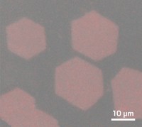
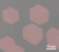
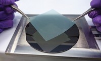
Graphene is one of the strongest known materials on the microscale. But some processes that could economically produce large quantities of graphene, such as chemical vapor deposition (CVD), create a polycrystalline version that is weak at the grain boundaries, the interfaces between variously oriented crystal regions that make up the bulk material. That weakness is a result of the processing, not an inherent characteristic of the material, report Gwan-Hyoung Lee, Ryan C. Cooper, Jeffrey W. Kysar, and James Hone of Columbia University and coworkers (Science 2013, DOI: 10.1126/science.1235126). Graphene is usually grown on copper foil, which must be etched away, and is transferred using a polymer support that is then removed. Both steps weaken the grain boundaries, making the material an order of magnitude weaker than pristine graphene, which has no grain boundaries. The group swapped the etching chemical and transfer method for gentler alternatives and, using an atomic force microscopy method called nanoindentation, found that the resulting films were nearly as strong as pristine graphene. With this information in hand, the group says CVD-prepared graphene can be used as “a large-area, high-strength material for flexible electronics” and in other applications.


Join the conversation
Contact the reporter
Submit a Letter to the Editor for publication
Engage with us on Twitter