Advertisement
Grab your lab coat. Let's get started
Welcome!
Welcome!
Create an account below to get 6 C&EN articles per month, receive newsletters and more - all free.
It seems this is your first time logging in online. Please enter the following information to continue.
As an ACS member you automatically get access to this site. All we need is few more details to create your reading experience.
Not you? Sign in with a different account.
Not you? Sign in with a different account.
ERROR 1
ERROR 1
ERROR 2
ERROR 2
ERROR 2
ERROR 2
ERROR 2
Password and Confirm password must match.
If you have an ACS member number, please enter it here so we can link this account to your membership. (optional)
ERROR 2
ACS values your privacy. By submitting your information, you are gaining access to C&EN and subscribing to our weekly newsletter. We use the information you provide to make your reading experience better, and we will never sell your data to third party members.
Materials
Toward Desktop Nanofabrication
Nanotechnology: Do-it-yourself lithography gets closer after two advances
by Bethany Halford
July 22, 2013
| A version of this story appeared in
Volume 91, Issue 29

Creating electronic gadgets such as smartphone components or microchip arrays for DNA analysis from the comfort of your desk just moved a little closer to reality, thanks to two advances in fabrication technology. These potential do-it-yourself methods for creating nanoscale patterns, one using heat and the other using light, could fundamentally change people’s lifestyles, researchers say.
“The modern micro- and nanofabrication industry relies on very expensive printing tools to produce all the electronic devices that we take for granted,” explains Chad A. Mirkin, the Northwestern University chemistry professor who led the research effort. By modifying existing lithography techniques, he says, it might be possible to give end users the capability to print electronic and other devices on demand.
One popular method of creating nanoscale patterns is to use scanning probe arrays, in which as many as 11 million tiny “pens” draw patterns. The problem with this approach, Mirkin notes, is that all the parts move in unison. “Anything you do with pen number one, you do with the other 10,999,999 pens.”
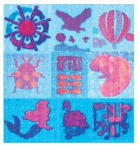
Mirkin’s team discovered that by placing microfabricated resistive heaters behind each pen, it’s possible to heat individual pens, causing them to move out of the plane to generate a specific feature (Proc. Natl. Acad. Sci. USA 2013, DOI: 10.1073/pnas.1311994110).
“Think of it as a dot matrix printer,” Mirkin explains. “We can take any dot matrix pattern and can tell the pens when to be engaged and when not to be engaged.” So, just one device can create multiple patterns.
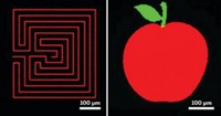
In the second advance, the team used mirrors to modify beam pen lithography, a technique that uses light to make patterns (Nat. Commun. 2013, DOI: 10.1038/ncomms3103). The researchers created a polymeric array of tiny pyramids and coated it with a thin layer of gold that light could not penetrate. They then used reactive ion etching to saw away the tip of each pyramid to create a tiny aperture that light can squeeze through to do lithography on the surface below. A digital mirror device, which takes one beam of light and splits it into 10,000, allows them to channel light through specific apertures to make a range of nanoscale patterns over the space of many square centimeters.
“We want to turn this into a true desktop fabrication tool—one that will do for electronics what the desktop printer did for printing,” Mirkin says.
“This is a massive integration of chemistry and mechanical engineering, and with engineering comes control and the ability to manufacture and fabricate,” comments Joseph M. DeSimone, a nanotechnology expert at the University of North Carolina, Chapel Hill, and North Carolina State University. “I think this kind of work is a quintessential example of research that can change people’s lives.”


Join the conversation
Contact the reporter
Submit a Letter to the Editor for publication
Engage with us on Twitter