Advertisement
Grab your lab coat. Let's get started
Welcome!
Welcome!
Create an account below to get 6 C&EN articles per month, receive newsletters and more - all free.
It seems this is your first time logging in online. Please enter the following information to continue.
As an ACS member you automatically get access to this site. All we need is few more details to create your reading experience.
Not you? Sign in with a different account.
Not you? Sign in with a different account.
ERROR 1
ERROR 1
ERROR 2
ERROR 2
ERROR 2
ERROR 2
ERROR 2
Password and Confirm password must match.
If you have an ACS member number, please enter it here so we can link this account to your membership. (optional)
ERROR 2
ACS values your privacy. By submitting your information, you are gaining access to C&EN and subscribing to our weekly newsletter. We use the information you provide to make your reading experience better, and we will never sell your data to third party members.
Materials
Silica Nanostructures Cut Power Demands Of Computer Memory
Electronics: Phase-change memory with low power needs could lead to fast data storage in personal electronics
by Kate Greene
March 14, 2013

Smart phones, tablets, and ultraslim laptops often store data in devices called flash memory. For years, engineers have worked on an alternative called phase-change memory that can read and write data a thousand times faster than flash memory. But even with companies such as Micron and Samsung working to commercialize the devices, progress has been slow. One reason is that phase-change memory consumes relatively large amounts of power. Now researchers have demonstrated a new device design involving silica nanostructures that uses just 5% of the power of traditional phase-change memory devices (ACS Nano, DOI: 10.1021/nn4000176).

Each phase-change memory cell is built like a sandwich: Electrodes on the top and bottom surround a glass-like material called a chalcogenide. Heat from the electrodes alters the structure of the chalcogenide, switching it between an amorphous, or glass-like, state and a crystalline one. The two states serve as the 0’s and 1’s of the stored data. The device can detect the different states because the amorphous state has a greater electrical resistance than the crystalline state.
The power problem pops up when the device resets the bits in each cell—converting the chalcogenide’s state from amorphous to crystalline. In this operation, the device melts the materials, a task that requires high currents, says Yeon Sik Jung, a professor of materials science and engineering at the Korea Advanced Institute of Science and Technology (KAIST).
Traditionally, researchers have decreased current requirements of phase-change memory by simply reducing the size of the cells. Smaller contact areas between the heating electrodes and the phase-change material allow for lower currents, Jung says.
But shrinking the devices leads to high production costs, he explains. To make the ever smaller cells, manufacturers must use new, expensive lithographic techniques.
Jung’s group and another KAIST team led by Keon Jae Lee developed a way to decrease power consumption, while relying on more established and less costly fabrication technologies. They added silica nanostructures between the heating electrodes and the chalcogenide. The structures act as insulators and block some contact between the two materials, effectively reducing the size of the device.
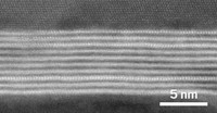
To form the nanostructures, the researchers add a layer of block copolymers, made of polystyrene and polydimethylsiloxane, between the heater and the chalcogenide, a film of Ge2Sb2Te5. Treating the devices with plasma then removes the polystyrene and converts the polydimethylsiloxane into silica. The team could produce nanostructures in multiple patterns and as small as 6 nm in width.
When the teams tested the devices, they found that their new designs required only 20% of the current to reset than the conventional design did. Jung points out that these are proof-of-concept tests: Their devices are 2 µm or 500 nm in size, while ones developed in industry are smaller than 30 nm. Still, Jung says that computer simulations suggest their approach will work in smaller devices.
Ritesh Agarwal, professor of material science and engineering at the University of Pennsylvania, calls the new design very interesting. The idea of effectively reducing the size of the device by using insulating nanostructures “is something people have not thought of before,” he says.


Join the conversation
Contact the reporter
Submit a Letter to the Editor for publication
Engage with us on Twitter