Advertisement
Grab your lab coat. Let's get started
Welcome!
Welcome!
Create an account below to get 6 C&EN articles per month, receive newsletters and more - all free.
It seems this is your first time logging in online. Please enter the following information to continue.
As an ACS member you automatically get access to this site. All we need is few more details to create your reading experience.
Not you? Sign in with a different account.
Not you? Sign in with a different account.
ERROR 1
ERROR 1
ERROR 2
ERROR 2
ERROR 2
ERROR 2
ERROR 2
Password and Confirm password must match.
If you have an ACS member number, please enter it here so we can link this account to your membership. (optional)
ERROR 2
ACS values your privacy. By submitting your information, you are gaining access to C&EN and subscribing to our weekly newsletter. We use the information you provide to make your reading experience better, and we will never sell your data to third party members.
Materials
Two-Dimensional Silicon Makes Its Device Debut
Materials: Silicene monolayers could help pave the way to faster, smaller electronics
by Matt Davenport
February 5, 2015
| A version of this story appeared in
Volume 93, Issue 6

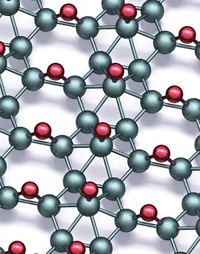
Researchers report that they’ve fabricated transistors made of a single layer of silicon atoms connected to three electrodes. These are the first functional devices to use two-dimensional silicon (Nat. Nanotechnol. 2015, DOI: 10.1038/nnano.2014.325).
Much like its all-carbon cousin, graphene, silicene promises an exciting array of electronic properties, according to theorists. Scientists believe both 2-D materials could form the basis of smaller, faster transistors—and, in turn, smaller, faster computers. But some argue silicene has the greater potential because the semiconductor industry already relies heavily on silicon.
“It’s inertia,” says Deji Akinwande of the University of Texas, Austin. An industry optimized for one material tends to stick with that material, explains Akinwande, who led the effort to build silicene transistors along with Alessandro Molle of the National Research Council of Italy.
Still, experimentalists have yet to fully characterize silicene’s electronic properties because the material is unstable. Silicon monolayers are so prone to bonding with oxygen and hydrogen that some researchers are still unconvinced that anyone has studied pure silicene. But the new transistors were produced with a method that could improve silicene’s stability and help further its experimental characterization.
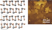
The team grew silicene by evaporating silicon atoms onto a smooth silver crystal. The researchers monitored silicene growth in real time using reflection high-energy electron diffraction and scanning tunneling microscopy. Once a 2-D monolayer was complete, they capped the silicene with a thin layer of alumina. Sandwiched between silver and alumina, the silicene remained stable for months, Akinwande says.
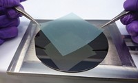
To complete the transistor, the team transferred the layered structure, alumina side down, to an oxidized silicon substrate that served as a back-gate electrode. Lastly, the team etched the exposed silver layer, generating two distinct pads to form the source and drain electrodes.
“To me, this is a very important study,” says Lok Lew Yan Voon, a physicist at The Citadel, in South Carolina. Lew Yan Voon, who was not involved in the study, was one of the researchers who named silicene in 2007. “This shows you can actually do something useful with the material,” he tells C&EN.
Yet it will likely be some time before silicene appears in any commercial semiconductor device. Once the researchers exposed silicene to air after etching the silver, their transistor degraded in a few minutes, limiting how thoroughly they could characterize the device or the material.
“The lack of compositional and structural characterization of the silicon material following its transfer to the device is concerning,” says Nathan P. Guisinger, a materials researcher at Argonne National Laboratory who was also not involved in the study. But Guisinger adds that he’s hopeful such work will lead to further studies and, ultimately, more robust characterization.
The team, however, says it was able to make a few measurements during the minutes-long window in which the silicene survived. For instance, the researchers found that silicene transistors conduct charge carriers almost as quickly as devices made from bulk silicon, Akinwande says. He adds that he’s optimistic that researchers can boost the material’s performance as they build more devices and grapple with instability problems.
Akinwande says, “If the stability issue is addressed at the device level, that will be revolutionary.”


Join the conversation
Contact the reporter
Submit a Letter to the Editor for publication
Engage with us on Twitter