Advertisement
Grab your lab coat. Let's get started
Welcome!
Welcome!
Create an account below to get 6 C&EN articles per month, receive newsletters and more - all free.
It seems this is your first time logging in online. Please enter the following information to continue.
As an ACS member you automatically get access to this site. All we need is few more details to create your reading experience.
Not you? Sign in with a different account.
Not you? Sign in with a different account.
ERROR 1
ERROR 1
ERROR 2
ERROR 2
ERROR 2
ERROR 2
ERROR 2
Password and Confirm password must match.
If you have an ACS member number, please enter it here so we can link this account to your membership. (optional)
ERROR 2
ACS values your privacy. By submitting your information, you are gaining access to C&EN and subscribing to our weekly newsletter. We use the information you provide to make your reading experience better, and we will never sell your data to third party members.
Materials
Nanowriting with conducting polymers
May 29, 2006
| A version of this story appeared in
Volume 84, Issue 22
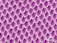
Molecularly ordered nanoscale patterns of conducting polymers can be prepared with high precision by using a scanning probe method, a new study reports (J. Am. Chem. Soc. 2006, 128, 6774). Scientists at the Naval Research Laboratory, Washington, D.C., and Georgia Institute of Technology developed a procedure in which a solid "ink"-—poly(3-dodecylthiophene) in this study-—is applied to a customized atomic force microscope cantilever that's equipped with a fast-acting tip heater. Referred to as thermal dip pen nanolithography, the method was used to pattern a silica surface with polymer structures measuring less than 100 nm in width and ranging in thickness (height) from a single monolayer (shown) to tens of monolayers. On the basis of single- and multilayered pattern thicknesses, the team concludes that the polymer structures are ordered with the alkyl groups perpendicular to the surface, an orientation that favors charge-carrier mobility.


Join the conversation
Contact the reporter
Submit a Letter to the Editor for publication
Engage with us on Twitter