Advertisement
Grab your lab coat. Let's get started
Welcome!
Welcome!
Create an account below to get 6 C&EN articles per month, receive newsletters and more - all free.
It seems this is your first time logging in online. Please enter the following information to continue.
As an ACS member you automatically get access to this site. All we need is few more details to create your reading experience.
Not you? Sign in with a different account.
Not you? Sign in with a different account.
ERROR 1
ERROR 1
ERROR 2
ERROR 2
ERROR 2
ERROR 2
ERROR 2
Password and Confirm password must match.
If you have an ACS member number, please enter it here so we can link this account to your membership. (optional)
ERROR 2
ACS values your privacy. By submitting your information, you are gaining access to C&EN and subscribing to our weekly newsletter. We use the information you provide to make your reading experience better, and we will never sell your data to third party members.
Materials
Wiring Electronics With Nanotubes
Nanoscale carbon wire offers advantages as an electronic material in displays, flexible electronics
by Bethany Halford
February 20, 2006
| A version of this story appeared in
Volume 84, Issue 8

As television sets evolve, so do the materials used to make them. The hottest TVs on the market now are flat-panel models. Consumer electronics retailers say plasma and liquid-crystal display (LCD) TVs were top sellers in 2005. And Corning, the world's largest maker of LCD glass, recently predicted that, in 2007, LCD TVs will account for 25% of all TVs sold.
As electronics makers watch flat-screen products' popularity and profits advance, a tiny problem continues to nag at them: The cost of indium tin oxide (ITO), a transparent conducting material integral to these devices, has surged in the past few years.
Indium, the raw material for ITO, is produced as a by-product of zinc mining. In 2003, 1 kg of indium cost $170, according to the U.S. Geological Survey. That price soared to $810/kg in 2005, driven by the demand for LCD and plasma displays.
The cost of ITO in an individual television doesn't amount to much: It's less than $1.00 for a 32-inch LCD display that retails for $1,300. But there have been threats of indium shortages, and ITO producers are worried about the reliability of the raw material supply.
Consequently, electronics makers have been eyeing other transparent conductive oxides and conducting polymers as potential ITO replacement materials. Another material, once considered too expensive and too impractical for consumer electronics, has started to look more and more promising: single-walled carbon nanotubes (SWNTs).
The nanotube's geometry and chemical bonding make it almost ideal in terms of charge-transport properties, according to George Gruner, a physics professor at the University of California, Los Angeles. The nanotube's mobility-the ease with which an electron moves through a material-is about 100 times greater than silicon's.
Integrating individual tubes into commercial electronic devices, however, has been trickier. Connecting components to an individual nanotube is too complex for mass-produced electronics. There's also the so-called chirality problem: SWNTs are always produced as a mixture of metallic and semiconducting structures, and semiconducting tubes usually outnumber metallic tubes by 2:1.
Several research groups, including Gruner's, have managed to circumvent these problems and transform carbon nanotubes into a viable ITO replacement material by making thin films from random networks of these nanoscale wires. Gruner likens the tangled networks to an interconnected freeway. Should an electron's route along one SWNT become blocked, it simply hops onto another nanotube and zips along.
"In thin films, you don't need to worry about spatial location or any individual tube," explains John A. Rogers, a chemistry and materials science professor at the University of Illinois, Urbana-Champaign, who is also developing nanotube-based electronics.
Materials makers can get around the chirality problem through statistical averaging. In low-density SWNT networks, Gruner explains, every conducting pathway interacts with a semiconducting tube, and these films function as semiconductors. At higher densities, there are more all-metallic pathways and the material essentially behaves like a metal. These higher density films can be used to make interconnects or gate electrodes.
Scientists working with nanotube networks point out that the material is also more versatile than both ITO and conducting polymers. "A random network of nanotubes will have very advantageous electronic and optical properties. It is going to be a transparent material, and it is going to be flexible," Gruner says.
Electronics manufacturers usually employ high temperatures to place ITO onto a substrate. That's a problem if you want to replace a glass substrate with plastic for lightweight, flexible electronics. Because SWNT networks don't require high-temperature processing, Gruner thinks SWNT networks will make the greatest impact in transparent flexible electronics.
"The main driving interest in nanotube networks would be for use on flexible plastic substrates," says Eric S. Snow, a scientist at the Naval Research Laboratory, Washington, D.C., who has developed nanotube-based sensors and is working on SWNT-based thin-film transistors. "The real economic driver behind that is the flat-panel display. Electronics makers would love to make laptop screens out of plastic because it would be lighter and more durable."
The processing methods developed in Gruner's lab involve dispersing commercially available SWNTs using solvents and surfactants and then printing or spraying the material onto a substrate. Controlling the film's density is critical in terms of how the material will be used, but Gruner says density is easy to control (Nano Lett. 2004, 4, 2513).
Gruner believes SWNT networks will find application opportunities in areas as diverse as solid-state lighting and electromagnetic shielding (Nano Lett. 2005, 5, 757). He and Northwestern University chemistry professor Tobin J. Marks have used the films to make anodes in organic light-emitting diodes. In collaboration with Michael D. McGehee of Stanford University and Niyazi Serdar Sariciftci of Johannes Kepler University, Linz, Austria, Gruner recently used the networks in a flexible solar cell that rivals solar cells made from ITO on glass.
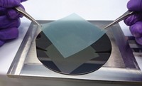
Rogers' group also works on solution-deposited tubes but currently focuses on a different method for incorporating nanotube networks into electronic devices. Rogers says that solution-deposited tubes often have poorer electrical properties than tubes grown directly on a substrate. So his group grows its own SWNT networks via chemical vapor deposition and then transfers the material onto a plastic substrate through a dry-transfer technique.
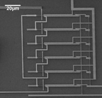
Using this method, Rogers recently fabricated a highly bendable, transparent thin-film transistor in which all the conducting and semiconducting components were made from SWNT networks (Adv. Mater. 2006, 18, 304). The transistor exhibits unique characteristics, such as extreme flexibility, that Rogers says would be difficult, or even impossible, to achieve with conventional materials.
Even with the success of his transistors made from random nanotube networks, Rogers thinks that SWNTs have much more to offer as an electronic material. "We want to see what the best performance you can possibly get from a nanotube is," he says. "We have our sights set on outperforming single-crystal silicon."
To that end, Rogers has been incorporating aligned arrays of SWNTs into thin-film transistors (Small 2005, 1, 1110). By using single-crystal quartz cut in a specific way as a growth substrate, Rogers produced large-scale, densely packed arrays of pristine nanotubes. The mobility of this material, when used as a semiconductor in a thin-film transistor, was substantially greater than that of the SWNT networks. The group also has managed to make transistors that use both random networks and aligned arrays of SWNTs.
There are, of course, challenges to creating SWNT-based electronic devices. Even though researchers have minimized the problems due to nanotube chirality, they haven't eliminated them entirely. "You can't wash out the fact that one-third of the tubes are metallic," Rogers acknowledges. "When implemented as a semiconductor thin film, some fraction of the metal tubes will be shorting your device out."
Gruner says one of his biggest challenges has been getting a reliable supply of SWNTs. He says the nanotube samples are frequently full of impurities and that the quality varies greatly from batch to batch, even from the same supplier. "There is a definite need for high-end nanotube suppliers," Gruner says.
"If you view this as a material, then we are probably at a stage where silicon was 60 years ago," Gruner reasons. "It was dirty and difficult to control. Then people started to make it cleaner and cleaner, and they started to dope it." That, he adds, is exactly what's happening with SWNT networks. The material is getting cleaner, less expensive, and easier to process. These are signs, he says, that it's in a strong competitive position among electronic materials.


Join the conversation
Contact the reporter
Submit a Letter to the Editor for publication
Engage with us on Twitter