Advertisement
Grab your lab coat. Let's get started
Welcome!
Welcome!
Create an account below to get 6 C&EN articles per month, receive newsletters and more - all free.
It seems this is your first time logging in online. Please enter the following information to continue.
As an ACS member you automatically get access to this site. All we need is few more details to create your reading experience.
Not you? Sign in with a different account.
Not you? Sign in with a different account.
ERROR 1
ERROR 1
ERROR 2
ERROR 2
ERROR 2
ERROR 2
ERROR 2
Password and Confirm password must match.
If you have an ACS member number, please enter it here so we can link this account to your membership. (optional)
ERROR 2
ACS values your privacy. By submitting your information, you are gaining access to C&EN and subscribing to our weekly newsletter. We use the information you provide to make your reading experience better, and we will never sell your data to third party members.
Materials
Intel Unveils New Transistor
Hafnium-based materials will be incorporated in 45-nm-technology chips
by Alexander H. Tullo
January 30, 2007
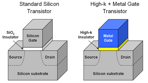
In what it dubs the "biggest change to computer chips in 40 years," Intel says it is using hafnium-based dielectric insulating materials with metal gates to construct the transistors in its new 45-nm-technology chips.
During those 40 years, silicon dioxide, the transistor dielectric material of choice, was made thinner and thinner to maintain adequate capacitance as chip size shrank. In the most advanced chips in production today, which have 65-nm circuit lines, the SiO2 layer is only 1.2 nm thick.
But making SiO2 thinner has also led to electrical leakage and excess heat. For the 45-nm transistor, Intel is replacing SiO2 with a hafnium-based material. With their higher dielectric constants, or k values, hafnium compounds form a thicker gate that blocks electrons while maintaining capacitance.
And because the new high-k dielectric material is not compatible with conventional silicon gate electrodes, Intel is using an unnamed metal as the gate electrode.
Intel says the new materials reduce transistor current leakage by more than 90% compared with SiO2. Successfully implementing 45-nm process technology permits a doubling of the transistor density on the chip.
"The implementation of high-k and metal materials marks the biggest change in transistor technology since the introduction of polysilicon gate MOS [metal-oxide-semiconductor] transistors in the late 1960s," Intel cofounder Gordon Moore said in a statement.
Intel isn't alone in using high-k materials to push chip size smaller. A day after Intel's announcement, IBM said it had successfully made transistors with an unspecified high-k and metal combination with partners Advanced Micro Devices, Sony, and Toshiba. IBM plans to incorporate its version of the new technology into chips next year.
But Intel intends to be the first on the market with commercial 45-nm-technology chips. The company is developing 15 45-nm processor products, five of which are being tested. The company intends to ramp up production of 45-nm-technology chips at facilities in Oregon and Arizona at the end of the year and in Israel by the first half of 2008.
Advertisement
You might also like...

The power is now in your (nitrile gloved) hands
Sign up for a free account to get more articles. Or choose the ACS option that’s right for you.
Already have an ACS ID? Log in
Join the conversation
Contact the reporter
Submit a Letter to the Editor for publication
Engage with us on Twitter