Advertisement
Grab your lab coat. Let's get started
Welcome!
Welcome!
Create an account below to get 6 C&EN articles per month, receive newsletters and more - all free.
It seems this is your first time logging in online. Please enter the following information to continue.
As an ACS member you automatically get access to this site. All we need is few more details to create your reading experience.
Not you? Sign in with a different account.
Not you? Sign in with a different account.
ERROR 1
ERROR 1
ERROR 2
ERROR 2
ERROR 2
ERROR 2
ERROR 2
Password and Confirm password must match.
If you have an ACS member number, please enter it here so we can link this account to your membership. (optional)
ERROR 2
ACS values your privacy. By submitting your information, you are gaining access to C&EN and subscribing to our weekly newsletter. We use the information you provide to make your reading experience better, and we will never sell your data to third party members.
Materials
Another One-Atom-Thick Material
Boron nitride joins graphene on list of thinnest free-standing crystals
by Mitch Jacoby
June 8, 2009
| A version of this story appeared in
Volume 87, Issue 23
Graphene isn't the only material capable of existing as a free-standing one-atom-thick film. The widely studied carbon material now shares that distinction with boron nitride, according to researchers in Germany (Nano Lett., DOI 10.1021/nl9011497).

Scientists had long predicted that single-atom-thick sheets of materials like graphene would spontaneously roll up into tubes or other curved structures if, indeed, the superthin films could be formed at all.
Just a few years ago, however, researchers showed that not only is it possible to separate atom-thick sheets of graphene from graphite, but it's also easy to do. That discovery touched off an explosion of studies that uncovered outstanding and potentially useful mechanical, electronic, and chemical properties of the thinnest material (C&EN, March 2, page 14). Now, atom-thick boron nitride films may be poised to share the spotlight with graphene.
Many other types of atom-thick monolayers have been grown on solid supports. But unlike graphene, other films generally cannot be separated intact from their supports.
Jannik C. Meyer, Ute Kaiser, and coworkers at the University of Ulm prepared microscopy samples of "hexagonal" boron nitride (h-BN) by peeling apart thin crystals of h-BN with adhesive tape—a method commonly used with graphene. Then, they transferred the few-atoms-thick flakes to a microscopy grid, a support that leaves relatively large sections of the flakes (millions of atoms) freely suspended over the grid holes.
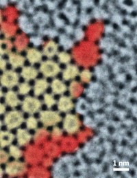
By exposing the sample to a transmission electron microscope beam, the team ejected atoms from the lattice and thinned the crystals to a single atomic layer. The group controlled the rate at which the beam whittled away the film by tuning the beam intensity and imaging conditions.
They were able to analyze the sputtering process by recording atomic-resolution images and videos. Among other findings, the team observed that the electron beam sweeps away one atomic layer at a time by forming triangular and polygon-shaped vacancies.
University of Manchester physicist Kostya S. Novoselov comments that this study provides insight into the mechanical properties and defect formation in boron nitride and marks "an important milestone in our understanding of the properties of two-dimensional crystals."


Join the conversation
Contact the reporter
Submit a Letter to the Editor for publication
Engage with us on Twitter