Advertisement
Grab your lab coat. Let's get started
Welcome!
Welcome!
Create an account below to get 6 C&EN articles per month, receive newsletters and more - all free.
It seems this is your first time logging in online. Please enter the following information to continue.
As an ACS member you automatically get access to this site. All we need is few more details to create your reading experience.
Not you? Sign in with a different account.
Not you? Sign in with a different account.
ERROR 1
ERROR 1
ERROR 2
ERROR 2
ERROR 2
ERROR 2
ERROR 2
Password and Confirm password must match.
If you have an ACS member number, please enter it here so we can link this account to your membership. (optional)
ERROR 2
ACS values your privacy. By submitting your information, you are gaining access to C&EN and subscribing to our weekly newsletter. We use the information you provide to make your reading experience better, and we will never sell your data to third party members.
Materials
More Materials Go 2-D
Graphene is joined by a growing collection of ultrathin crystals with new properties and applications
by Mitch Jacoby
October 8, 2012
| A version of this story appeared in
Volume 90, Issue 41
\

\
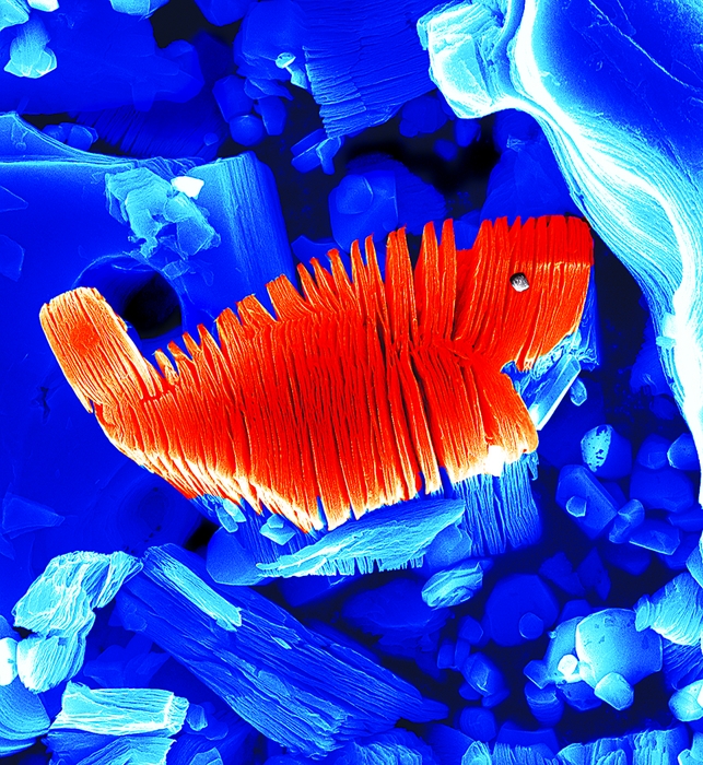
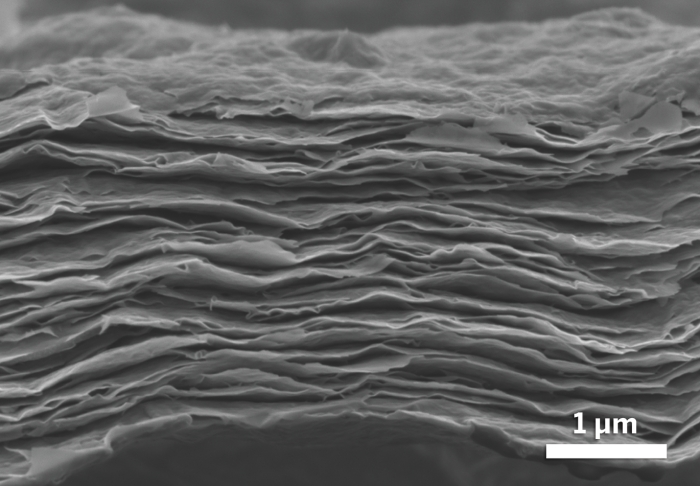
A simple acid treatment selectively etches the Al layers from materials such as Ti3AlC2, leaving stacks of separable Ti3C2 sheets. The central particle in each of these SEM images, which have been colored strictly for aesthetics, is roughly 10 μm wide.
With its atomic thinness and outstanding electronic and mechanical properties, graphene stormed the materials research world about five years ago, repeatedly grabbing headlines in the mainstream and scientific press alike. Large numbers of scientists set about probing this one- or few-atoms-thick form of carbon and devoted themselves to developing its applications. Clearly, this nearly two-dimensional (2-D) material is fascinating. But when it comes to atomically thin or nearly atomically thin materials, graphene isn’t the only game in town.
The past few years—and especially the past few months—have seen several materials, including boron nitride, molybdenum disulfide, metal carbides, and others, join the 2-D club. Researchers are investigating the fundamental properties of these materials and devising methods for preparing them in large quantities. One of the main goals of this work is to exploit the chemical, electronic, and other unique properties of this group of ultrathin materials for applications for which graphene is not ideal.
Joining the 2-D materials club requires more of materials than simply being one (or a few) atomic or molecular layers thin. They must also be isolable and able to support themselves physically. Many types of films have been prepared as monolayers on solids but cannot be separated intact from their supports.
Graphene stole the materials spotlight because it can be manipulated, moved around, and poked and prodded with devices that measure electronic and mechanical properties of isolated films. In addition, and rather importantly, vanishingly thin flakes of graphene can be transferred to microscopy grids, holey supports that leave relatively large sections of the flakes (millions of atoms) freely suspended over the grid holes.
The early work with graphene earned physicists Andre K. Geim and Konstantin S. Novoselov, both of the University of Manchester, in England, the 2010 Nobel Prize in Physics (C&EN, Oct. 11, 2010, page 8). But even as the Manchester team published its highly cited graphene findings in Science in 2004 (DOI: 10.1126/science.1102896), it was already gearing up to lay the groundwork for studies of several other 2-D crystals such as boron nitride, MoS2, and NbSe2.
In work published the following year, the researchers showed that rubbing these layered materials against solids chips off very thin flakes, as they had found for graphite. Those flakes can often be thinned further to a few or even a single molecular layer by pressing them into an adhesive tape sandwich and repeatedly peeling apart the tape (Proc. Natl. Acad. Sci. USA, DOI: 10.1073/pnas.0502848102).
That method provided Jannik C. Meyer and Ute Kaiser, electron microscopy specialists at the University of Ulm, in Germany, with a few-atoms-thick crystal of a form of boron nitride known as hexagonal-BN. In an electron microscopy experiment that probed the material’s mechanical properties and its tendency to incur lattice damage, the team used the microscope’s electron beam to whittle away a hexagonal BN crystal to a single atomic layer while recording atomic-resolution images and videos of the process. The study revealed a decomposition mechanism in which the electron beam sweeps away one atomic layer at a time by forming triangular and polygon-shaped vacancies.
More recently, Yury Gogotsi and Michel W. Barsoum, materials science professors at Drexel University, showed that Ti3AlC2, a three-component layered material, can be chemically exfoliated—peeled apart—by treating powders of the compound with hydrofluoric acid solution at room temperature. The treatment selectively etches aluminum, Barsoum explains, yielding 2-D sheets composed of a few molecular layers of Ti3C2. The research group, which includes Drexel graduate student Michael Naguib and coworkers at Linköping University, in Sweden, published their findings last year in Advanced Materials (DOI: 10.1002/adma.201102306).

The back story behind the Drexel team’s discovery isn’t obvious from the group’s publications. But Barsoum is quick to share it. He explains that the group was looking to make anodes for lithium-ion batteries that outlast standard graphite anodes, which physically degrade as batteries are subjected to repeated charge-discharge cycles. On the basis of their earlier studies, the Drexel researchers identified a family of electrically conducting robust carbides and nitrides as promising anode materials. The compounds are known as the MAX phases, where M refers to an early transition metal, A symbolizes main-group elements such as Al and Si, and X represents C or N.
By treating the compounds with acid solution, the group aimed to selectively remove some of the atoms from Ti3AlC2 and other MAX phases. The goal was to make room in the anode lattice for Li ions to reversibly insert themselves during battery charging and discharging. Initial structural analysis of the acid-treated products showed that the procedure worked well, Barsoum says. Next, the group conducted preliminary electrochemistry tests, which also yielded encouraging results.
At that point, the researchers analyzed their samples in detail and discovered that the simple acid treatment had completely removed the Al layers and exfoliated the crystals into 2-D sheets of Ti3C2. Excited by their findings, the group labeled the new 2-D materials MXenes (pronounced “maxenes”) to denote the loss of the A element and emphasize the materials’ graphenelike 2-D morphology.
“Never in our wildest dreams did we think it would be that easy to make 2-D materials,” Barsoum exclaims. “But at that point, we knew we were potentially onto something big.” Ti3AlC2 is just one example of a MAX phase, Barsoum points out. The family includes some 60 members.
In a follow-up study published this year, the Drexel team reported that seven other MAX phases were exfoliated via acid treatment. The starting materials include Ti2AlC, Ta4AlC3, (Ti0.5Nb0.5)2AlC, (V0.5Cr0.5)3AlC2, and Ti3AlCN (ACS Nano, DOI: 10.1021/nn204153h). And in collaboration with the research group of materials science professor Patrice Simon, of Paul Sabatier University in France, the Drexel team conducted detailed electrochemistry tests to evaluate Ti2C’s performance as an anode material in Li-ion batteries designed for rapid charging and discharging. The key finding in that study is that the material retained its charge capacity during 1,000 rapid charging cycles (J. Electrochem. Soc., DOI: 10.1149/2.003208jes).
“Our goal is to find new 2-D materials that have unique and useful properties that are different from graphene’s,” Gogotsi says. “We produced seven new materials. Dozens more are possible.” He goes on to say that the surface chemistry and other properties of MXenes are expected to be different from one another and from those of graphene. “We may have opened up a whole new playground for chemists, materials scientists, and others who are interested in this area.”

One property of graphene that limits its application is the lack of a band gap, a property that makes it possible for an electron to be promoted from a material’s occupied valence band to its unoccupied conduction band. Band gaps are a defining feature of semiconductors and a required property of materials from which digital circuits are fashioned.
For that reason, Han Wang, Tomás Palacios, and coworkers at Massachusetts Institute of Technology are turning to materials such as MoS2 to make ultrathin digital circuits. MoS2 and related materials such as WSe2 and WS2 are endowed with band gaps and can be prepared as lightweight flexible films that are nearly atomically thin. The materials are being studied for use in flexible and foldable display systems that can be supported on paper, plastics, textiles, and the surfaces of other common materials.
Just recently, the MIT group fabricated complex integrated circuits on a single piece of MoS2 just two molecular layers thick (Nano Lett., DOI:
The team used lithography methods and vapor deposition techniques to deposit various types of metal electrodes and isolated them from one another with insulating films of hafnium oxide. Through these methods, they built tiny transistors in which the MoS2 film served as the channel material, a key transistor component. The group connected up to a dozen transistors to produce several types of logic circuits, including inverter and five-stage ring oscillator devices.
“These are exciting times in electronics,” Wang says. A lot of new materials are coming up, and that presents many new opportunities and challenges.
Manchester’s Geim expresses a similar view. The expanding library of 2-D crystals can be used where and when the need arises, as indicated by application, he says. The recent progress in the field fills him with optimism. “This is going to fly high sooner rather than later,” he says.
You might also like...


The power is now in your (nitrile gloved) hands
Sign up for a free account to get more articles. Or choose the ACS option that’s right for you.
Already have an ACS ID? Log in
Join the conversation
Contact the reporter
Submit a Letter to the Editor for publication
Engage with us on Twitter