Advertisement
Grab your lab coat. Let's get started
Welcome!
Welcome!
Create an account below to get 6 C&EN articles per month, receive newsletters and more - all free.
It seems this is your first time logging in online. Please enter the following information to continue.
As an ACS member you automatically get access to this site. All we need is few more details to create your reading experience.
Not you? Sign in with a different account.
Not you? Sign in with a different account.
ERROR 1
ERROR 1
ERROR 2
ERROR 2
ERROR 2
ERROR 2
ERROR 2
Password and Confirm password must match.
If you have an ACS member number, please enter it here so we can link this account to your membership. (optional)
ERROR 2
ACS values your privacy. By submitting your information, you are gaining access to C&EN and subscribing to our weekly newsletter. We use the information you provide to make your reading experience better, and we will never sell your data to third party members.
Materials
Bendable Silicon Electronics
Materials: Exfoliation technique converts rigid silicon devices into flexible ones
by Prachi Patel, special to C&EN
February 20, 2014
| A version of this story appeared in
Volume 92, Issue 8

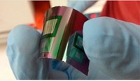
By shaving off an ultrathin layer from the top of a silicon wafer, researchers can transform rigid electronic devices into flexible ones (ACS Nano 2014, DOI: 10.1021/nn405475k). The new method is more cost-effective than similar techniques, its developers say.
Engineers are working on flexible circuitry in hopes of developing wearable electronics or displays that can roll up. To achieve the high performance of silicon circuits in flexible devices, a few research groups have started fabricating electronics on rigid silicon wafers and then slicing off the thin surface layer carrying the components. These slices can bend when added to a plastic film.
But these techniques require either expensive forms of silicon or costly processing steps that involve nonstandard fabrication methods, says Muhammad M. Hussain at King Abdullah University of Science & Technology, in Saudi Arabia. His group’s new process uses standard techniques and works with monocrystalline silicon, a relatively inexpensive and common form of silicon.
After fabricating devices on a wafer, the researchers deposit a thin silicon dioxide film over the entire surface. Using photolithography and reactive ion etching, the team next bores 5-µm-wide pores in the oxide film and the underlying silicon. They then expose the wafer to xenon difluoride gas. It passes through the pores and etches away a layer of silicon micrometers below the wafer’s surface to release the ultrathin top layer carrying the devices.
By polishing the leftover wafer, the researchers can reuse the silicon for repeat fabrication and exfoliation steps. This enables them to make six 25- to 50-µm-thick slices from a 0.5-mm-thick wafer.
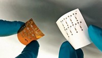
The team has used the process to make bendable capacitors, transistors, lithium-ion batteries, and devices that convert heat into electricity. The devices are flexible enough that researchers could wrap them around the edge of a 0.5-mm-thick silicon wafer.
John A. Rogers at the University of Illinois, Urbana-Champaign, calls the new slicing process a clever way to “create thin, wispy sheets of high-quality electronics.” This and similar peel-off methods will find a niche once flexible electronics take off, says Joachim N. Burghartz at the University of Stuttgart, in Germany.


Join the conversation
Contact the reporter
Submit a Letter to the Editor for publication
Engage with us on Twitter