Advertisement
Grab your lab coat. Let's get started
Welcome!
Welcome!
Create an account below to get 6 C&EN articles per month, receive newsletters and more - all free.
It seems this is your first time logging in online. Please enter the following information to continue.
As an ACS member you automatically get access to this site. All we need is few more details to create your reading experience.
Not you? Sign in with a different account.
Not you? Sign in with a different account.
ERROR 1
ERROR 1
ERROR 2
ERROR 2
ERROR 2
ERROR 2
ERROR 2
Password and Confirm password must match.
If you have an ACS member number, please enter it here so we can link this account to your membership. (optional)
ERROR 2
ACS values your privacy. By submitting your information, you are gaining access to C&EN and subscribing to our weekly newsletter. We use the information you provide to make your reading experience better, and we will never sell your data to third party members.
Materials
Hard Silicon Wafers Yield Flexible Electronics
Electronics: New silicon exfoliation technique converts rigid electronic devices into ones that could be worn or rolled up
by Prachi Patel
February 14, 2014

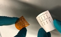
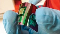
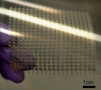
By shaving off an ultrathin layer from the top of a silicon wafer, researchers have transformed rigid electronic devices into flexible ones (ACS Nano 2014; DOI: 10.1021/nn405475k). The shaving process could be used to fabricate parts for wearable electronics or displays that can roll up. Compared to similar techniques to make bendable silicon electronics, the new method is more cost-effective and produces more flexible devices, its developers say.
Typically, engineers fabricate flexible electronics with organic semiconductors laid down on plastic. But these organic components don’t perform as well as traditional silicon circuits, which are built on rigid wafers up to 0.5 mm thick.
To achieve the high performance of silicon circuits in flexible devices, a few research groups have started fabricating electronics on silicon wafers and then slicing off the thin surface layer carrying the components. Unfortunately, these techniques require either expensive forms of silicon or costly processing steps that use nonstandard fabrication methods, says Muhammad M. Hussain, an electrical engineer at the King Abdullah University of Science & Technology, in Saudi Arabia. Also, the existing slicing methods waste material, because the silicon wafer can’t be reused once the top layer has been peeled off, he says.
Hussain and his colleagues developed a new process that starts with a monocrystalline silicon wafer, the most common form of silicon used by the electronics industry. The researchers make devices on it using typical lithographic methods.
To slice the silicon, the researchers first deposit a thin silicon dioxide film over the entire wafer, in part to protect the fabricated devices during the slicing process. They use photolithography and reactive ion etching to make 5-µm-wide pores that tunnel through the oxide film and about 20 µm into the underlying silicon. Then the team exposes the wafer to xenon difluoride gas that passes through the pores and etches away a layer of silicon micrometers below the wafer’s surface. This etching releases the ultrathin top layer carrying the devices.
The researchers can polish the remaining wafer and reuse it to make another set of devices. A 0.5-mm-thick wafer can yield six 25- to 50-µm-thick silicon slices, Hussain says. The team has used the process to make bendable capacitors, transistors, lithium-ion batteries, and devices that convert heat into electricity. The devices are flexible enough to wrap around the edge of a 0.5-mm-thick silicon wafer.
Hussain and his colleagues have developed a similar process to make flexible devices using polycrystalline and amorphous silicon, which are also common in the electronics industry. He says his team is now building memory and computer logic devices to combine with the battery and electricity generator to make the first silicon-based wearable computer.
John A. Rogers, a materials scientist at the University of Illinois, Urbana-Champaign, calls the new slicing process a clever way to “create thin, wispy sheets of high-quality electronics, suitable for mounting on lightweight, flexible sheets of plastic.”
Joachim N. Burghartz at the University of Stuttgart, in Germany, who has developed a technique to create flexible silicon devices, says that this and other peel-off methods will find a niche once flexible electronics take off.


Join the conversation
Contact the reporter
Submit a Letter to the Editor for publication
Engage with us on Twitter