Advertisement
Grab your lab coat. Let's get started
Welcome!
Welcome!
Create an account below to get 6 C&EN articles per month, receive newsletters and more - all free.
It seems this is your first time logging in online. Please enter the following information to continue.
As an ACS member you automatically get access to this site. All we need is few more details to create your reading experience.
Not you? Sign in with a different account.
Not you? Sign in with a different account.
ERROR 1
ERROR 1
ERROR 2
ERROR 2
ERROR 2
ERROR 2
ERROR 2
Password and Confirm password must match.
If you have an ACS member number, please enter it here so we can link this account to your membership. (optional)
ERROR 2
ACS values your privacy. By submitting your information, you are gaining access to C&EN and subscribing to our weekly newsletter. We use the information you provide to make your reading experience better, and we will never sell your data to third party members.
Materials
New Reagents For Atomic Layer Deposition
Tailored ALD precursors form atomically thin layers of metals, dielectrics, and other compounds
by Mitch Jacoby
August 17, 2015
| A version of this story appeared in
Volume 93, Issue 32

Making films one molecular layer at a time might seem like painstaking work limited to laboratories researching esoteric surface science.
But it’s not.
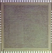
Atomic layer deposition (ALD), a layer-at-a-time film-growth method, has been growing by leaps and bounds in recent years. The technique produces films that are exceptionally uniform and conformal, meaning the films closely follow the contours of irregularly shaped objects. Because of these properties, the method is widely used by the semiconductor industry to manufacture electronic circuit components. ALD has also proved in numerous laboratory demonstrations to be a versatile method for making catalysts, materials for energy production and storage, films for flexible displays, and several other types of advanced functional materials.
Unlike other deposition processes, ALD is based on a set of carefully choreographed surface chemical reactions. Typically, films are grown by exposing a surface to alternating pulses of two vapor-phase reagents, A and B. The reagents, usually referred to as precursors, react sequentially with the surface to form a binary product. Each A-B cycle increases the film thickness by one molecular layer.
“The enabler in ALD is definitely chemistry,” says Harvard University chemist Roy G. Gordon, a thin-film specialist. Much of that chemistry has been applied to making films of metal oxides such as Al2O3, HfO2, and TiO2. Gordon and other thin-film experts have been working to extend the technique to grow thin films of many other types of compounds—and that means identifying or designing chemical reagents with exactly the right combination of properties for the task. Some of the latest findings on new ALD precursors were highlighted last month in Portland, Ore., at an international conference sponsored by AVS, a science and technology organization that focuses on materials research.
To kick off the meeting, Intel’s Michael C. Mayberry, a corporate vice president and global research director, enumerated some of the semiconductor industry’s needs and anticipated uses for ALD. He noted that one broad class of electronics applications requires “thin conformal films of metallic materials.” He explained that the films are used as interconnections between circuit components and for tuning the minimum amount of energy needed to remove an electron from a material.
No surprise then that several research teams have been examining ALD chemistry for growing metal films, especially of copper, a good electrical conductor. For example, Atsushi Sakurai, a research manager with Tokyo-based Adeka, which supplies ALD reagents, reported on his company’s progress with proprietary copper precursors based on aminoalkoxides with the general form Cu[OCH(R)CH2NR′R″]2.
To be useful for ALD, in Sakurai’s view, the precursor should exhibit high vapor pressure and a low melting point, and the ALD reaction should proceed at a temperature that’s low enough to prevent the metal from clumping in the deposited film. Further, it should be possible to synthesize the compound at large scale, in high purity, and at reasonable cost.
Sakurai stressed that Adeka’s copper aminoalkoxides fit the bill. His group has made high-quality copper films at low temperature by reacting the compounds with hydrogen from a low-energy hydrogen plasma. The company is also evaluating iminoalkoxides of cobalt and nickel for making films of those metals.
Depositing thin films of copper is one thing. Making the metal stay put is quite another. “Copper has a nasty habit of diffusing if it’s not encapsulated with a protective barrier,” Gordon said. Running electric current through the tiny wires that interconnect transistors and other circuitry causes copper atoms to start migrating out of the wires, which eventually can lead to chip failure.
To head off that process, manufacturers devised non-ALD ways of encasing nanosized copper wires with a tantalum nitride-like film. The films are currently 4 to 5 nm thick. But that 20-year-old solution appears to have run its course. To keep up with the general shrinking of chip components over time, electronics manufacturers need to reduce the size of these encased wires, and they can’t shrink the copper itself. Unlike transistors, which operate faster and use less power as they shrink to the low nanoscale range, metal wires become more resistant and transmit signals more slowly. But the manufacturers can’t make the tantalum nitride films thinner because below a certain size they no longer offer much protection against copper diffusion.
Gordon thinks ALD can help solve this problem. His group has developed an ALD process for making manganese silicate, a material that prevents copper diffusion at a film thickness of less than 2 nm. The chemistry is based on a reaction between a manganese amidinate compound and a silanol with tert-butoxy groups or other organic ligands. Gordon noted that there are other non-ALD ways to make manganese silicate films. But the Harvard group’s ALD method offers greater control over deposition and higher uniformity in chemical composition.
ALD’s ability to make highly uniform films may also be useful for improving other circuit components such as capacitors. These charge-storage devices are ubiquitous and are found in consumer electronics, hybrid electric vehicles, and many other applications.


One way to boost a capacitor’s charge-storage capacity and lifetime is to coat the charge-storing plates at the heart of these devices with a thin-film material that exhibits an exceptionally high dielectric constant at thicknesses of just a few nanometers. Barium titanate (BaTiO3) seems like a promising candidate, but making high-quality films at low temperatures has been challenging.

At the Portland meeting, Shinjita Acharya reported on a proprietary barium pyrrole compound developed by BASF that is compatible with low-temperature ALD. Acharya is a postdoctoral researcher working with Stanford University mechanical engineer Friedrich B. Prinz, whose group is collaborating with BASF.
To make thin films, the Stanford group first formed a layer of barium oxide by reacting the barium pyrrole with a pulse of water. Then they added a layer of titania by using another set of ALD reactions. By repeating the process and keeping the film-support warm, the group built up layers of BaO and TiO2 that diffused into each other. The result was a microscopically smooth and uniform BaTiO3 film with good electrical properties.
Acharya and other speakers at the Portland meeting stressed that ALD is a versatile method for making films of exceptional quality and wide-ranging chemical composition. To enable the method to reach its potential, Mayberry remarked, “we need creative chemical researchers to design new precursors and coreactants.” ALD also needs vendors dedicated to providing high-quality precursors, and it needs engineers who can teach ALD instruments “to do new tricks,” he said. “The future is bright when we rise to these needs.”


Join the conversation
Contact the reporter
Submit a Letter to the Editor for publication
Engage with us on Twitter