Advertisement
Grab your lab coat. Let's get started
Welcome!
Welcome!
Create an account below to get 6 C&EN articles per month, receive newsletters and more - all free.
It seems this is your first time logging in online. Please enter the following information to continue.
As an ACS member you automatically get access to this site. All we need is few more details to create your reading experience.
Not you? Sign in with a different account.
Not you? Sign in with a different account.
ERROR 1
ERROR 1
ERROR 2
ERROR 2
ERROR 2
ERROR 2
ERROR 2
Password and Confirm password must match.
If you have an ACS member number, please enter it here so we can link this account to your membership. (optional)
ERROR 2
ACS values your privacy. By submitting your information, you are gaining access to C&EN and subscribing to our weekly newsletter. We use the information you provide to make your reading experience better, and we will never sell your data to third party members.
Surface Chemistry
Mechanochemistry etches silicon one layer at a time
Scanning probe method may sharpen microfabrication dexterity
by Mitch Jacoby
April 30, 2018
| A version of this story appeared in
Volume 96, Issue 18
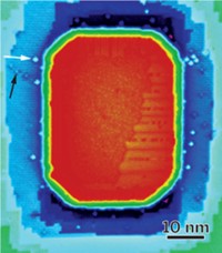
Mechanical forces induced by a scanning probe tip can trigger chemical reactions that selectively remove a single atomic layer of silicon (Nat. Commun. 2018, DOI: 10.1038/s41467-018-03930-5). The finding may lead to ways of etching electronic materials with atomic precision, a level of control needed to further shrink today’s circuit components, which already sport nanoscale features. By fitting a scanning probe tip with a silica sphere and slowly moving it against a crystalline silicon surface in humid air, Xinchun Lu of Tsinghua University, Seong H. Kim of Pennsylvania State University, and coworkers methodically picked off silicon layers one at a time without inducing subsurface damage. Using microscopy, surface chemical analysis, and molecular dynamics simulations the group determined that as the surfaces start to come into contact, they react with water present at the interface, forming Si-O-H groups on silica and Si-H groups on silicon. As the probe tip slides, it bridges the modified groups on both surfaces by forming an Si-O-Si bond, which starts to break the Si-Si bond in silicon. In the final stage, the Si-Si bond breaks, transferring a silicon atom to the silica surface. Control tests indicate that this etching process is not caused by mechanical wear and does not occur in the absence of water or when the silica tip is replaced with other materials.


Join the conversation
Contact the reporter
Submit a Letter to the Editor for publication
Engage with us on Twitter