Advertisement
Grab your lab coat. Let's get started
Welcome!
Welcome!
Create an account below to get 6 C&EN articles per month, receive newsletters and more - all free.
It seems this is your first time logging in online. Please enter the following information to continue.
As an ACS member you automatically get access to this site. All we need is few more details to create your reading experience.
Not you? Sign in with a different account.
Not you? Sign in with a different account.
ERROR 1
ERROR 1
ERROR 2
ERROR 2
ERROR 2
ERROR 2
ERROR 2
Password and Confirm password must match.
If you have an ACS member number, please enter it here so we can link this account to your membership. (optional)
ERROR 2
ACS values your privacy. By submitting your information, you are gaining access to C&EN and subscribing to our weekly newsletter. We use the information you provide to make your reading experience better, and we will never sell your data to third party members.

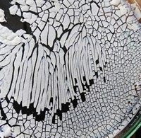
David Mills discovered this pocked landscape upon taking a close look at the surface of a silicon sample with a scanning electron microscope. As part of a project examining laser ablation of silicon, Mills, a facilities manager at Queen Mary University of London, placed the material under an ultraviolet laser pulse. The laser was strong enough to vaporize some of the atoms on the silicon’s surface. While the silicon atoms floated around as vapor, they reacted with gaseous hydrogen chloride that Mills had added to the experiment. The acidic HCl molecules reacted with the silicon vapor, and then the reaction products settled back down on the surface, creating this rough pattern. As a result, the silicon got very black because the textured surface absorbs more light than the original smooth crystalline surface.
Submitted by David Mills
Do science. Take pictures. Win money. Enter our photo contest here.
Related C&EN Content:


Join the conversation
Contact the reporter
Submit a Letter to the Editor for publication
Engage with us on Twitter