Advertisement
Grab your lab coat. Let's get started
Welcome!
Welcome!
Create an account below to get 6 C&EN articles per month, receive newsletters and more - all free.
It seems this is your first time logging in online. Please enter the following information to continue.
As an ACS member you automatically get access to this site. All we need is few more details to create your reading experience.
Not you? Sign in with a different account.
Not you? Sign in with a different account.
ERROR 1
ERROR 1
ERROR 2
ERROR 2
ERROR 2
ERROR 2
ERROR 2
Password and Confirm password must match.
If you have an ACS member number, please enter it here so we can link this account to your membership. (optional)
ERROR 2
ACS values your privacy. By submitting your information, you are gaining access to C&EN and subscribing to our weekly newsletter. We use the information you provide to make your reading experience better, and we will never sell your data to third party members.
Electronic Materials
The first fully printed electronics roll off printers ready to use
Low-temperature aerosol jet printing process builds transistors on paper and plastic
by Prachi Patel, special to C&EN
October 7, 2019

Interest in printed electronics has surged in the past decade as a way to mass produce RFID tags and sensors at low cost. But printing digital logic devices on a substrate today involves multiple steps beyond the printer, such as rinsing or curing in an oven. Now, researchers have made the first fully printed transistors—ones that emerge from a printer with all of their components in place, ready to be used (ACS Nano 2019, DOI: 10.1021/acsnano.9b04337).
Work on printed circuitry typically has focused on inkjet printers, which use tiny nozzles to deposit ink droplets onto a substrate. The inks are suspensions of different materials—conductive nanoparticles, semiconducting carbon nanotubes, or insulating polymers—used to print different layers of thin-film transistors over several runs through the printer. But after printing, the process requires washing away unwanted materials and heating at high temperature to cure the insulating layer.
To get rid of those extra steps, Aaron D. Franklin, an electrical and computer engineer at Duke University, and his colleagues used a technique called aerosol jet printing. Their new process allows all of the steps to happen in place at the printer. Everything is done at temperatures less than 80 °C, which lets the researchers print transistors on paper.
Aerosol jet printing uses pressure and an inert gas to break up the ink into microscopic droplets “like aerosol hair spray,” Franklin says. “This makes it possible to print in smaller lines and to dry more rapidly because you are minimizing droplet size and the volume of background solvent.” That means less unwanted material to rinse off or evaporate outside a printer.

The team first printed layers of carbon nanotubes on paper and plastic substrates to form the conductive channel of a transistor. Without removing the substrate from the printer, the researchers placed a few drops of toluene for 20 s on the substrate, gently warmed it at 80 °C, and blow-dried it with a nitrogen gun to remove excess material. Then they printed electrodes using water-based silver nanowire ink.
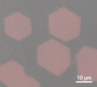
The next layer marked a key advance: printing a quality insulator film using an ink of 2-D hexagonal boron nitride (h-BN) flakes. “One of the most challenging areas for printed logic devices has been the development of a good, patterned insulator layer,” says Ioannis Kymissis, an electrical engineer at Columbia University who was not involved in the work.
Printed h-BN layers normally require baking at 180 °C for 2 h to create a smooth film with flat, well-arranged flakes that gives good insulating properties. And a critical concern is to avoid the mixing of the h-BN inks with the silver nanowire inks above and below, which would lead to defective transistors.
To overcome these problems, the Duke engineers added hydroxypropyl methylcellulose to their h-BN ink, which makes the ink thicker and keeps it from mixing with the silver nanowire layer below. The process, to their surprise, gave high-quality insulating h-BN layers that did not blend with the silver nanowires and did not need heating. The researchers believe the binder helps the microdroplets spread out and stick to the surface, laying down the flakes in a structured way as they are being printed. “This is an exciting discovery,” Franklin says.
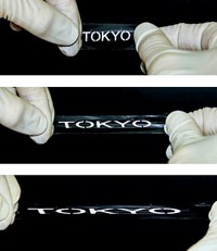
Finally, the researchers printed the last electrode layer on top of the insulator and then tested the devices using standard current-voltage measurements. The devices maintained their performance after being bent 1,000 times.
The aerosol jet printing process isn’t fast enough for high-volume manufacturing, but it could be used to make custom, on-the-fly electronics or paper-based sensors. The method could also print biomolecules, Franklin says, to create a customized array of biosensors on an electronic bandage for monitoring a patient.
The fully printed, mechanically flexible devices show “outstanding overall performance,” Kymissis says, “and pulling all of this together makes for a significant advance in the field.”


Join the conversation
Contact the reporter
Submit a Letter to the Editor for publication
Engage with us on Twitter