Advertisement
Grab your lab coat. Let's get started
Welcome!
Welcome!
Create an account below to get 6 C&EN articles per month, receive newsletters and more - all free.
It seems this is your first time logging in online. Please enter the following information to continue.
As an ACS member you automatically get access to this site. All we need is few more details to create your reading experience.
Not you? Sign in with a different account.
Not you? Sign in with a different account.
ERROR 1
ERROR 1
ERROR 2
ERROR 2
ERROR 2
ERROR 2
ERROR 2
Password and Confirm password must match.
If you have an ACS member number, please enter it here so we can link this account to your membership. (optional)
ERROR 2
ACS values your privacy. By submitting your information, you are gaining access to C&EN and subscribing to our weekly newsletter. We use the information you provide to make your reading experience better, and we will never sell your data to third party members.
Nanomaterials
Electroadhesive stamp assembles tiny electronic components
Carbon nanotube–based material can arrange nanoparticles in precise configurations
by Kerri Jansen
October 19, 2019
| A version of this story appeared in
Volume 97, Issue 41
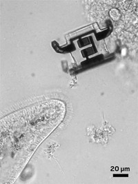
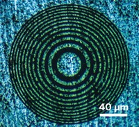
Small electronic parts like circuit boards and display components are often assembled using robotic grippers that can place multiple elements into precise configurations. But advances in electronics are demanding ever-smaller components, and there’s a limit to how far traditional mechanical grippers can be miniaturized. At very small scales, surface forces tend to dominate, presenting a challenge to picking up and placing objects by traditional means. So scientists are looking for alternatives to help assemble objects at tiny scales. Researchers at the Massachusetts Institute of Technology, the Korea Advanced Institute of Technology, and the University of Pennsylvania have developed a nanotube-based, voltage-activated surface that lets them manipulate objects as small as 20 nm wide without requiring heat or chemical reactions (Sci. Adv. 2019, DOI: 10.1126/sciadv.aax4790). The stamp is made of vertically aligned carbon nanotubes coated in aluminum oxide, a dielectric material. When a small voltage is applied, the stamp electrostatically attracts the target object. Once the object is moved into place, researchers can release it by turning off the voltage. The researchers varied the density of tubes and thickness of coating to achieve a high on-off ratio of stickiness. They used the stamp to pick up and arrange silver nanowires, polymer and metal nanoparticles, and light-emitting diode chiplets.


Join the conversation
Contact the reporter
Submit a Letter to the Editor for publication
Engage with us on Twitter