Advertisement
Grab your lab coat. Let's get started
Welcome!
Welcome!
Create an account below to get 6 C&EN articles per month, receive newsletters and more - all free.
It seems this is your first time logging in online. Please enter the following information to continue.
As an ACS member you automatically get access to this site. All we need is few more details to create your reading experience.
Not you? Sign in with a different account.
Not you? Sign in with a different account.
ERROR 1
ERROR 1
ERROR 2
ERROR 2
ERROR 2
ERROR 2
ERROR 2
Password and Confirm password must match.
If you have an ACS member number, please enter it here so we can link this account to your membership. (optional)
ERROR 2
ACS values your privacy. By submitting your information, you are gaining access to C&EN and subscribing to our weekly newsletter. We use the information you provide to make your reading experience better, and we will never sell your data to third party members.
Nanomaterials
To shrink electronics further, innovative chemical deposition methods may save the day
Researchers experiment with area-selective atomic layer deposition to precisely place layers of conducting and insulating materials within circuits
by Mitch Jacoby
June 8, 2018
| A version of this story appeared in
Volume 96, Issue 24

Credit: ZhiHua Chen | At Stanford University, Stacey F. Bent (from left), Dara Bobb-Semple, and Tzu-Ling Liu devise strategies for making ALD a spatially selective tool for growing thin films.
In brief
Through clever innovations in photolithography, the semiconductor industry has steadily made circuitry smaller, faster, and more powerful. The decades-old approach to downsizing may soon run out of steam. To continue marching onward to electronics with ever-smaller features, researchers are devising chemical means to deposit ultrathin layers of molecules in precise locations within microelectronic circuits. One technique, known as area-selective atomic layer deposition (ALD), offers ways to lay down films of electrical conductors and insulators from the bottom up, with extreme spatial precision. The method’s success rests on innovative ways of selectively activating one nanosized surface region for ALD chemistry while deactivating a neighboring area.
Imagine trying to paint the sharp edge rather than the flat face of every blade of grass in a little garden patch—without leaving a dab of paint anywhere else. That’s roughly the gargantuan challenge facing microelectronics manufacturers today.
For decades, manufacturers have steadily shrunk electronic circuits, thereby creating mobile phones and other devices that are ever faster and more powerful. But the time-honored technique they’ve been using to accomplish these feats—top-down lithography—depends on masks and photoresists for patterning and numerous deposition and etching steps to transform bulk silicon wafers into ever-smaller electronic structures. And that method is now running up against the limits of what it can do.
Transistors in today’s microelectronics already sport structures such as electrodes with 10-nm dimensions, and 7-nm circuit components are now making their way into high-volume manufacturing, according to Dennis M. Hausmann, a senior staff scientist at Lam Research, which makes semiconductor processing equipment. To reach the next frontier, 5 nm and below, device manufacturers will need to figure out how to paint those blades of grass.
In their case, the blades are tightly spaced semiconductor structures, and the paint is a layer of electrically conducting or insulating material placed just so. The chemical strategy they’re pursuing to grow these structures from the bottom up is called area-selective atomic layer deposition (ALD).
“We are witnessing a significant transformation driven by the semiconductor industry’s need to supplant physically driven photolithography patterning methods with new chemically driven patterning methods,” says Gregory N. Parsons, a vapor deposition specialist at North Carolina State University.
Basic ALD science has been around since the 1970s, but in the past 10 years or so, the deposition method has taken off commercially, and its popularity has soared. Variations on ALD, such as the new area-selective strategy, are drumming up even more excitement for the technique and its promise.
Silvia Armini, a senior scientist at Belgium-based IMEC, an R&D organization specializing in microchip technology, concurs.
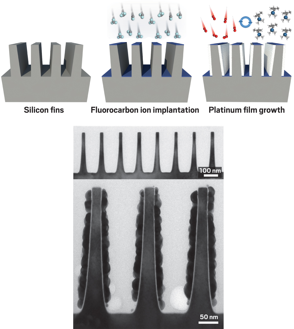
To selectively apply a metal film to the vertical walls of a nanoelectronic device containing silicon fins (left), researchers deactivate the horizontal regions via ion implantation (middle, blue), then use multiple cycles of a pair of ALD reactions to deposit platinum (right, white). Micrographs recorded before (top) and after (bottom) ALD confirm the method works.
To selectively apply a metal film to the vertical walls of a nanoelectronic device containing silicon fins (top), researchers deactivate the horizontal regions via ion implantation (middle, blue), then use multiple cycles of a pair of ALD reactions to deposit platinum (bottom, white). Micrographs recorded before (micrograph, top) and after (micrograph, bottom) ALD confirm the method works.
Area-selective ALD is rapidly gaining interest because of its potential in advanced fabrication schemes for next-generation nanoelectronics, she says. The strong sensitivity of ALD to surface chemistry makes it particularly appealing.
Compared with other film-growth methods, ALD stands out as an ideal technique for generating films that are exceptionally uniform and conformal, meaning the coatings it produces closely follow the contours of complex and irregularly shaped objects.
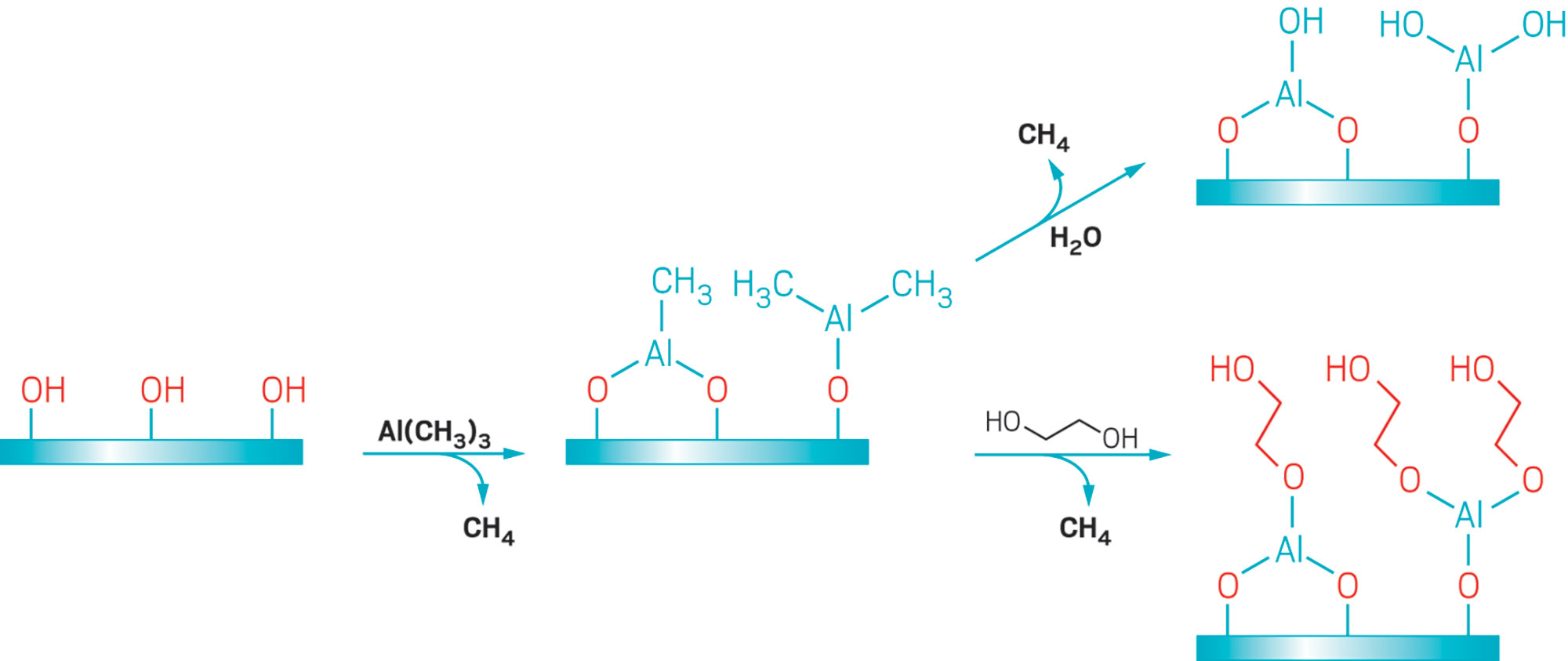
To carry out ALD is to run a pair of sequential surface reactions. Scientists first deliver a pulse of reagent A to a surface. This reagent reacts selectively with one type of functional group on the substrate. The reaction automatically stops after all the functional groups have reacted. Scientists then pump away excess reagent A, following up with a pulse of reagent B. This reagent reacts selectively with the functional groups left behind by the reaction with A. One A-B cycle deposits one molecular layer of a metal oxide or other compound. Repeating the cycle adds a second layer, and so forth.
Area-selective ALD takes the method to the next level. To control precisely where on surfaces ALD films grow, scientists are using beams of ions, electrons, and other creative means to modify surface properties of some nanosized regions in microelectronics while leaving adjacent ones unaffected. The procedures selectively turn on or turn off ALD chemistry only in the modified regions.
More than 150 enthusiastic scientists from 10 countries gathered at NC State in Raleigh last month to learn about the latest developments in this new field. The workshop, which was organized by Parsons and endorsed by AVS, a materials science and technology organization, drew nearly 60% of its attendees from industry, an indication of the high level of commercial interest.
Although some suppliers of ALD equipment claim that device makers widely use ALD to make today’s products, those companies closely guard details of their manufacturing processes. It’s no secret, however, that the R&D divisions of all major microelectronics companies are heavily involved in ALD method development.
One way to control where ALD films grow is to make some regions of a substrate more hydrophilic or hydrophobic than neighboring areas. That property can be exploited to selectively attract or repel one of the ALD reagents and thereby inhibit reactions at the modified spots.
Dara Bobb-Semple, Stacey F. Bent, and coworkers at Stanford University have used this approach to selectively decorate some faces of a three-dimensional structure known as a silicon fin array, but not others. Manufacturers use multiple processing steps to convert these structures, which look like a series of fins aligned parallel to one another and mounted on a horizontal base, into modern nanoelectronic components called FinFETs, or fin field-effect transistors. Like all transistors, billions of which are included in a single mobile phone, FinFETs function as fast-acting switches. Device makers recently switched from a two-dimensional transistor design to the 3-D fin design to make FETs smaller and faster. Further reductions in FinFET dimensions will challenge manufacturers’ ability to accurately deposit the layers of conductors and insulators needed to make these devices operate properly. Area-selective ALD might help.
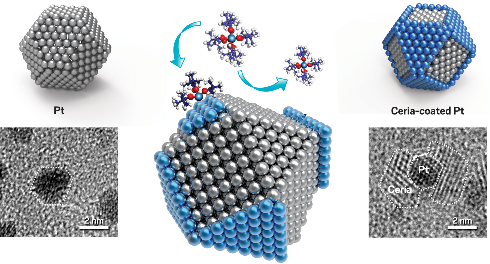
Surface energy differences between facets of a platinum nanoparticle (left) cause a ceria precursor molecule to bind to Pt(111) facets but not to (100) facets (middle), leaving just the (111) facets covered with ceria (middle and right, blue). Transmission electron microscopy images confirm selective deposition.
Surface energy differences between facets of a platinum nanoparticle (top) cause a ceria precursor molecule to bind to Pt(111) facets but not to (100) facets (middle), leaving just the (111) facets covered with ceria (middle and bottom, blue). Transmission electron microscopy images confirm selective deposition.
To demonstrate the method’s potential, the Stanford team directed a beam of energetic fluorocarbon ions at the fin structure. Because the researchers angled the beam so that it came down perpendicular to the fin array, the ions could strike and slightly penetrate only the horizontal surfaces of the array’s structures—the tops of the fins and the flat surfaces between them—rendering those surfaces hydrophobic. The vertical walls of the silicon substrate weren’t affected.
Then the team sequentially used a methylcyclopentadienyl platinum compound and air (oxygen) as ALD reagents to grow platinum films. Because the horizontal surfaces of the fin arrays were hydrophobic, when the arrays were enveloped with the reagents, the platinum compound did not bind there: It stuck only to the vertical walls. This kind of selective deposition of conducting layers represents one of the steps needed to turn silicon fins into working circuit components (ACS Nano 2016, DOI: 10.1021/acsnano.6b00094).
A more common way to control where ALD occurs on a surface is with self-assembled monolayers (SAMs). By patterning regions of a surface with SAMs of molecules containing long alkyl tails, scientists can also render parts of a surface hydrophobic and selectively inhibit ALD film growth. The Stanford researchers compared the ion implantation method they used on the FinFET structure with this SAM technique and found the ion strategy is simpler, more widely applicable, and much faster.
Another approach that scientists are taking with area-selective ALD is precisely activating nanosized surface regions rather than deactivating them. Steven M. George’s research group at the University of Colorado, Boulder, does its patterning with an electron beam, and as George reported at last month’s workshop, his group used the method to grow films of boron nitride on select portions of a nanosized 3-D silicon “trench structure.” Manufacturers routinely encounter that shape, which resembles the interior of an egg carton, while carrying out the long series of processing steps used for making various types of memory and logic circuit components.
As with the ion implantation method, this electron-beam-based technique affects only the surface regions within its line of sight—in this case, horizontal surfaces. The basis of the effect, however, is completely different. The Colorado team perpendicularly directed the electrons at a hydrogen-capped silicon surface. The impact drives away the hydrogen via a process known as electron-stimulated desorption and exposes silicon dangling bonds—reactive sites with unfilled valencies. That leaves the horizontal trench surfaces ripe for ALD.
To grow BN films, the researchers deliver a pulse of borazine (B3N3H6), which readily bonds to the active sites, then follow the borazine with another shot of electrons. This time the electrons drive hydrogen out of borazine. That process causes the residue to coalesce and form a single molecular layer of boron nitride with a graphenelike structure. Subsequent borazine-electron cycles add additional BN layers.
The study shows that BN, which is prized for its thermal stability and hardness and has been used as the insulating layer in FETs constructed entirely from 2-D materials, can be deposited with fine spatial control via an electron-driven process. The study also shows that ALD can grow the films at 100 °C and lower, which is more than 500 °C cooler than is possible with other deposition methods. The lower processing temperatures could benefit temperature-sensitive substrates (J. Phys. Chem. C 2018, DOI: 10.1021/acs.jpcc.8b00796).
Still another way to carry out area-selective ALD is to let nature choose where to grow ALD films rather than artificially activate or deactivate surface regions. At Huazhong University of Science & Technology (HUST), Rong Chen and coworkers found that intrinsic differences in the surface energies of various nanoparticle facets, or crystal faces, can cause an ALD reagent to preferentially bind to one facet over another. That selectivity causes the product ALD film to grow on the preferred facet. That’s like spray painting a set of nanosized dice and ensuring that only the even-numbered faces are coated.
The group applied its finding to a model catalytic system—ceria-coated platinum nanoparticles. Many large-scale chemical processes depend on metal nanoparticles supported on metal oxides. As these kinds of catalysts age, small particles often coalesce into larger ones, burying catalytic sites in the interiors of the larger particle and causing a drop in catalytic activity. Protective coatings sometimes mitigate the coalescence, or sintering, problem, but they can block reagent molecules from reaching catalytic sites.
The HUST team prepared custom-made catalysts to study the problem. The researchers used an organocerium compound and ozone as deposition reagents and showed that the ceria film produced via ALD selectively grows on Pt(111) crystal faces and leaves the (100) faces bare. Then they evaluated the catalysts’ ability to mediate CO oxidation—a key reaction in engine-emissions cleanup.
Their tests showed that Pt nanoparticles decorated with thin patches of ceria were more active than uncoated ones and exhibited improved resistance to sintering up to 700 °C (Small 2017, DOI: 10.1002/smll.201700648). ALD’s facet-dependent chemistry
Advertisement
may also benefit microelectronics. The materials in the HUST study, a metal-oxide insulator and a metallic conductor, are used throughout electronics manufacturing. And silicon and other semiconductors are known to exhibit facet-dependent chemical and physical properties.
Many of the presentations at the Raleigh workshop ended with session chairs having to cut off questions and proposing that speakers and attendees continue their lively discussions offline. And discuss they did. The meeting was filled with enthusiastic researchers talking shop in every corner of the conference center.
The broad collection of ALD advances unveiled last month represents just the tip of the iceberg in this developing field of spatially controlled film growth. But it suggests a high level of interest.
“People have been talking about top-down versus bottom-up fabrication for a long time, mostly speculating about how it might manifest,” NC State’s Parsons says. “We’re finally beginning to witness this innovative transition unfold. It’s exciting to see.”
You might also like...


The power is now in your (nitrile gloved) hands
Sign up for a free account to get more articles. Or choose the ACS option that’s right for you.
Already have an ACS ID? Log in
Join the conversation
Contact the reporter
Submit a Letter to the Editor for publication
Engage with us on Twitter