Advertisement
Grab your lab coat. Let's get started
Welcome!
Welcome!
Create an account below to get 6 C&EN articles per month, receive newsletters and more - all free.
It seems this is your first time logging in online. Please enter the following information to continue.
As an ACS member you automatically get access to this site. All we need is few more details to create your reading experience.
Not you? Sign in with a different account.
Not you? Sign in with a different account.
ERROR 1
ERROR 1
ERROR 2
ERROR 2
ERROR 2
ERROR 2
ERROR 2
Password and Confirm password must match.
If you have an ACS member number, please enter it here so we can link this account to your membership. (optional)
ERROR 2
ACS values your privacy. By submitting your information, you are gaining access to C&EN and subscribing to our weekly newsletter. We use the information you provide to make your reading experience better, and we will never sell your data to third party members.
Nanomaterials
Micromachine Writes Calligraphy With Atoms
Nanotechnology: A low-cost, moving stencil can direct evaporated atoms onto a surface, drawing complex nanopatterns
by Louisa Dalton
July 3, 2013

Engineers have devised many clever methods for creating nanoscale patterns on surfaces. But most current options for creating these precise features, such as electron beam nanolithography, are either expensive or limited to shapes that can be made with stencils.
Now, David J. Bishop, a physicist at Boston University, and his coworkers have put together an inexpensive microscale machine that can direct atoms onto a surface in a controlled manner (Nano Lett. 2013, DOI: 10.1021/nl401699w). The device—which acts as a moving stencil—can lay down such precise, complex patterns that the technique is akin to writing with atoms, Bishop says.
Bishop’s team wanted to find ways around the limitations with current nanoscale patterning techniques. For example, nanoscale stencils, which often sit motionless, can’t produce shapes that have holes, such as rings or loops. Another technique called dip pen nanolithography uses the tip of an atomic force microscope to direct a flow of material onto a surface, like ink from a pen. It can produce a wide range of features but works only with liquid inks.
In the new technique, the researchers heat a material inside a vacuum chamber and allow the evaporated atoms to rain down onto a surface. They designed a microelectromechanical machine that moves a stencil and a shutter to control and direct that stream of atoms.
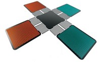
Their machine consists of two thin polysilicon plates. The first plate is rectangular with a 20-μm-diameter hole. It slides back and forth, acting like a shutter for the flow of atoms from the evaporator. The atoms move through the first plate’s hole and reach the second round plate, which is pierced in the center with an array of holes of different sizes and shapes. The holes allow a thin stream of atoms to flow through and range from hundreds of nanometers to less than 50 nm in size. The round plate is tethered to four electromechanical springs that can shift the plate in any direction over the surface that the researchers want to write on. When the moving pinholes align with the shutter, the atoms pass through both holes and stick to a silicon-nitride surface underneath.

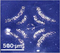
The researchers can draw patterns, including rings and infinity symbols, by programming how and when the holes align. They tested the technique with gold and chromium atoms, but it should be compatible with any material that can be heated and evaporated, Bishop says. He thinks the technique should be able to drop just one atom at a time, but the team hasn’t yet measured that capability.
The micromachines don’t cost much to make, Bishop says. The scientists order the polysilicon plates from a commercial foundry at low cost and then use a focused ion beam to pierce the nanosized holes in the plates. The micromachines are so cheap, Bishop says, that the team can experiment with one, throw it out, and “go get another clean one—for a dollar or two.”
With controlled atom-writing, Bishop hopes to study how properties of matter such as ferromagnetism and superconductivity manifest themselves in very small groups of atoms.
Jürgen Brugger, a nanotechnology researcher at the Swiss Federal Institute of Technology in Lausanne, says the micromachine will allow researchers to study novel materials and devices because of its ability to create tapered thin films and unique nanoelectronic devices. But he thinks the technique’s greatest advantage is its low-cost fabrication, which makes it far more accessible than other nanopatterning tools like electron-beam writers.


Join the conversation
Contact the reporter
Submit a Letter to the Editor for publication
Engage with us on Twitter