Advertisement
Grab your lab coat. Let's get started
Welcome!
Welcome!
Create an account below to get 6 C&EN articles per month, receive newsletters and more - all free.
It seems this is your first time logging in online. Please enter the following information to continue.
As an ACS member you automatically get access to this site. All we need is few more details to create your reading experience.
Not you? Sign in with a different account.
Not you? Sign in with a different account.
ERROR 1
ERROR 1
ERROR 2
ERROR 2
ERROR 2
ERROR 2
ERROR 2
Password and Confirm password must match.
If you have an ACS member number, please enter it here so we can link this account to your membership. (optional)
ERROR 2
ACS values your privacy. By submitting your information, you are gaining access to C&EN and subscribing to our weekly newsletter. We use the information you provide to make your reading experience better, and we will never sell your data to third party members.
Materials
Advancing toward Finer Circuitry
Carbon nanotubes incorporated into Si chips; nanowires grown on a virus
by Bethany Halford
January 12, 2004
| A version of this story appeared in
Volume 82, Issue 2
Two recently published papers describe advances on the road to nanocircuitry using two key device components--carbon nanotubes and inorganic nanowires.
A group led by Jeffrey Bokor and Yu-Chih Tseng from the electrical engineering department at the University of California, Berkeley, and Hongjie Dai and Ali Javey from Stanford University's chemistry department has made the first working circuit that incorporates both carbon nanotubes and standard silicon technology [Nano Lett., published online Dec. 19, 2003, http://dx.doi.org/10.1021/nl0349707]. Bokor says combining ubiquitous silicon circuitry with the nascent technology to create hybrid electronics will make it easier to introduce carbon nanotube products into the market.
The team uses chemical vapor deposition (CVD) to grow single-walled carbon nanotubes onto "islands" of an iron catalyst on the circuit platform. This technique of nanotube synthesis is incompatible with most silicon circuitry because it must be done at high temperatures--875 C in this case--that would melt the copper components commonly used in electronic chips. So the group replaced copper with molybdenum, which can take the heat.
As a proof of principle, the researchers designed the circuit so that the conductivity of each of its 2,000 nanotubes can be assessed individually. This strategy allows the researchers to determine whether a particular nanotube has metallic or semiconducting properties, because CVD tends to give mixtures of the two types of tube. Carbon nanotube makers can therefore use the circuit as a practical tool for determining the ratio of metallic to semiconducting nanotubes from a CVD preparation.
"That's crucial information for learning how to better control the growth of carbon nanotubes," Bokor tells C&EN.
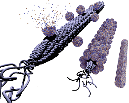
The second nanotech advance has emerged from the union of molecular biology and materials science. Materials science professor Angela M. Belcher and graduate student Daniel J. Solis at Massachusetts Institute of Technology and postdoc Chuanbin Mao at the University of Texas, Austin, spearheaded an effort to make magnetic and semiconducting nanowires using a virus-based scaffold [Science, 303, 213 (2004)].
The group uses an evolutionary screening process to find peptides that can control various features of inorganic nanoparticle nucleation. Then they genetically engineer the pencil-shaped M13 bacteriophage so that the virus's capsid incorporates a specific peptide on the surface of its shaft. The desired inorganic compound nucleates at the peptide sites and becomes ordered onto the virus scaffold. High-temperature annealing removes any organic materials, leaving the inorganic particles to collapse into the space formerly occupied by the virus to form a nanowire.
"We're trying to develop this as a general kit to make wires out of many different materials," Belcher tells C&EN. The group has already made single-crystal, semiconducting ZnS and CdS nanowires, as well as ferromagnetic CoPt and FePt nanowires.
Belcher also would like to make more complex materials using this general DNA modification method. Her group recently made two different genetic modifications to the same M13 bacteriophage, one at the "eraser" end and one at the "pencil tip" end. They then linked the two ends together with another molecule to form a nanoring [Nano Lett., published online Dec. 16, 2003, http://dx.doi.org/10.1021/nl0347536].
You might also like...


According to Belcher, growing nanowires on viruses allows one to use milder (aqueous, ambient, nontoxic) conditions than required by other nanowire fabrication methods.
The power is now in your (nitrile gloved) hands
Sign up for a free account to get more articles. Or choose the ACS option that’s right for you.
Already have an ACS ID? Log in
Join the conversation
Contact the reporter
Submit a Letter to the Editor for publication
Engage with us on Twitter