Advertisement
Grab your lab coat. Let's get started
Welcome!
Welcome!
Create an account below to get 6 C&EN articles per month, receive newsletters and more - all free.
It seems this is your first time logging in online. Please enter the following information to continue.
As an ACS member you automatically get access to this site. All we need is few more details to create your reading experience.
Not you? Sign in with a different account.
Not you? Sign in with a different account.
ERROR 1
ERROR 1
ERROR 2
ERROR 2
ERROR 2
ERROR 2
ERROR 2
Password and Confirm password must match.
If you have an ACS member number, please enter it here so we can link this account to your membership. (optional)
ERROR 2
ACS values your privacy. By submitting your information, you are gaining access to C&EN and subscribing to our weekly newsletter. We use the information you provide to make your reading experience better, and we will never sell your data to third party members.
Materials
Organic Layer Smooths Dielectric Films
Insulating layer in nanoelectronic devices benefits from an organic undercoat
by Mitch Jacoby
May 30, 2011
| A version of this story appeared in
Volume 89, Issue 22
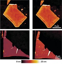
Depositing a few layers of organic molecules on graphene enables subsequently deposited oxide layers to be grown without imperfections, according to a study published in ACS Nano (DOI: 10.1021/nn201414d). The investigation identifies a fabrication step that can improve the quality of insulating layers crucial to the performance of graphene-based electronic devices. To exploit graphene for use as a field-effect transistor electrode, this ultrathin carbon film needs to be selectively coated with smooth, thin, and defect-free layers of insulating materials known as high-k dielectrics. Graphene’s hydrophobicity and inertness, however, prevent dielectrics such as alumina and hafnia from being deposited on graphene smoothly and uniformly. Some surface treatments have been shown to improve the deposition process, but they tend to degrade graphene’s structure and electronic properties. A team of researchers, led by Northwestern University’s Mark C. Hersam, has shown that those problems can be overcome by growing one or two monolayers of a perylene dianhydride compound, PTCDA, on graphene before depositing films of alumina and hafnia. According to the team, surface analysis and electrical measurements show that dielectric films grown that way are highly uniform and conformal, and that the graphene remains undamaged.


Join the conversation
Contact the reporter
Submit a Letter to the Editor for publication
Engage with us on Twitter