Advertisement
Grab your lab coat. Let's get started
Welcome!
Welcome!
Create an account below to get 6 C&EN articles per month, receive newsletters and more - all free.
It seems this is your first time logging in online. Please enter the following information to continue.
As an ACS member you automatically get access to this site. All we need is few more details to create your reading experience.
Not you? Sign in with a different account.
Not you? Sign in with a different account.
ERROR 1
ERROR 1
ERROR 2
ERROR 2
ERROR 2
ERROR 2
ERROR 2
Password and Confirm password must match.
If you have an ACS member number, please enter it here so we can link this account to your membership. (optional)
ERROR 2
ACS values your privacy. By submitting your information, you are gaining access to C&EN and subscribing to our weekly newsletter. We use the information you provide to make your reading experience better, and we will never sell your data to third party members.
Materials
Graphene Stacks Grown With Controlled Thickness
Nanomaterials: Chemical vapor deposition produces large sheets of multilayer graphene
by Prachi Patel
November 16, 2012

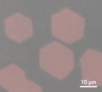
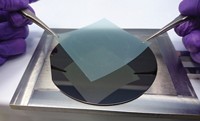
Researchers have found a straightforward way to grow large pieces of multilayer graphene and to control their thickness (ACS Nano, DOI: 10.1021/nn303328e). Producing films with a precise number of layers could enable graphene-based transistors and other devices, the researchers say.
While single layers of graphene conduct charge more efficiently than silicon can, the material lacks a band gap, an electronic property necessary in devices such as transistors. But researchers have found that graphene films consisting of two layers stacked in a certain way have a small band gap when a voltage crosses the material.
The two layers in these films stack such that every other carbon atom in the six-carbon rings of the top graphene layer sits over the middle of the hexagonal space created by a six-carbon ring of the bottom layer. This arrangement is called Bernal stacking. Researchers have suggested that three- and four-layer graphene sheets would have different electronic properties that are attractive for applications.
So far, scientists have obtained multilayer graphene sheets only occasionally, using sticky tape, while trying to exfoliate single layers from pieces of graphite. “Once in a while you rip off bilayer graphene that is Bernal stacked,” says Rice University chemist James M. Tour. These flakes are only micrometers wide, so the process could never yield practical-sized sheets of the materials, he says.
Tour and his colleagues, including his graduate students Zhengzong Sun and Abdul-Rahman O. Raji, wanted to find a way to use chemical vapor deposition (CVD) to produce Bernal-stacked films with controlled thicknesses. CVD, which can produce centimeters-wide graphene sheets, involves growing graphene on copper foil inside a pressure-controlled glass chamber. Chemists fill the chamber with a mix of hydrogen and methane, which is the source of carbon.
Through trial and error, Sun and Raji found that they could control the number of graphene layers by tuning the pressure in the chamber, while keeping constant the pressure ratio of hydrogen to methane. In separate trials, they increased the total pressure from 5 to 760 torr, while keeping the pressure ratio of hydrogen to methane at 28 to 1.
As the pressure increased, thicker graphene films grew on the copper surface. The researchers made films from one- to more than 10-layers thick. Bilayer graphene formed at 93.3 torr, while trilayer and tetralayer formed at 152 and 277.6 torr, respectively. The researchers used high-resolution transmission electron microscopy and electron diffraction, respectively, to confirm the number of layers in the materials and that the bilayer sheets achieved Bernal stacking. They also created a transistor with the bilayer material and measured its electronic properties.
Alberto Morpurgo, a physicist at the University of Geneva, in Switzerland, says this study is the first he has seen to use chemical vapor deposition to grow graphene with a precise number of layers. He points out that the team needs to present more data to confirm that their films have uniform thickness and stacking patterns. Nevertheless, growing large areas of Bernal-stacked, multilayer graphene could enable electronic applications, he says.


Join the conversation
Contact the reporter
Submit a Letter to the Editor for publication
Engage with us on Twitter