Advertisement
Grab your lab coat. Let's get started
Welcome!
Welcome!
Create an account below to get 6 C&EN articles per month, receive newsletters and more - all free.
It seems this is your first time logging in online. Please enter the following information to continue.
As an ACS member you automatically get access to this site. All we need is few more details to create your reading experience.
Not you? Sign in with a different account.
Not you? Sign in with a different account.
ERROR 1
ERROR 1
ERROR 2
ERROR 2
ERROR 2
ERROR 2
ERROR 2
Password and Confirm password must match.
If you have an ACS member number, please enter it here so we can link this account to your membership. (optional)
ERROR 2
ACS values your privacy. By submitting your information, you are gaining access to C&EN and subscribing to our weekly newsletter. We use the information you provide to make your reading experience better, and we will never sell your data to third party members.
Return to the article: 2-D materials go beyond graphene
The 2-D world
Scientists have developed five groups of 2-D materials from elements across the periodic table.
MXenes (Ti3C2, Ta4C3, and others) - Xenes (B, Si, P, Ge, and Sn) - Transition metal dichalcogenides (MoS2, WS2, and others) - Organic materials (C) - Nitrides (GaN, BN, and Ca2N)
MXenes
Ti3C2, Ta4C3, and others
Description: A family of transition metal carbides, carbonitrides, and nitrides prepared from layered precursors.
Properties & potential applications: Scientists have made nearly 30 MXenes based on Sc, Ti, Zr, Hf, V, Nb, Ta, Cr, and Mo—including mixed-metal examples. The materials' high strength, flexibility, conductivity, and chemical tunability make them promising candidates for applications in energy storage, electromagnetic shielding, tough composites, and water purification.
Key citation: Nat. Rev. Mater. 2017, DOI: 10.1038/natrevmats.2016.98

In a new family of 2-D materials called MXenes, one type of transition metal (M ́, red or purple) sandwiches a metal carbide (green or yellow) containing a second transition metal (M ́). The outer layers are capped with O, F, and OH surface groups (blue and brown).
Borophene
B
Description: A buckled sheet of boron atoms arranged in a honeycomb pattern.
Properties & potential applications: Owing to its electron deficiency, boron forms numerous polymorphs, most of which are semiconductors. The 2-D form, borophene, is a metal-like conductor, which could be useful for energy-storage devices and fast electronics.
Key citations:
Science 2015, DOI: 10.1126/science.aad1080
Angew. Chem. Int. Ed. 2015, DOI: 10.1002/anie.201509285
Angew. Chem. Int. Ed. 2015, DOI: 10.1002/anie.201505425

These structural models depict the 2-D layer of one type of borophene (top) and a top and side view of a 2-D layer of a different type (bottom).
Silicene
Si
Description: A buckled sheet of silicon atoms arranged in a honeycomb pattern.
Properties & potential applications: Silicene's band-gap and charge-transport characteristics coupled with silicon's ubiquity in the semiconductor world make silicene an attractive material for fast transistors and other electronics.
Key citation: Nat. Nanotechnol. 2015, DOI: 10.1038/nnano.2014.325
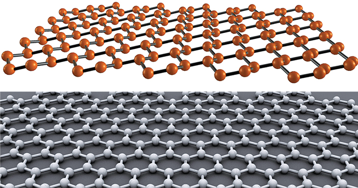
Silicene's buckled structure (top) compared with a flat graphene crystal.
Stanene
Sn
Description: A buckled sheet of tin atoms arranged in a honeycomb pattern.
Properties & potential applications: Stanene has a large band gap and a unique conductivity profile—it's a so-called topological insulator. This combination of properties may lead to applications in thermoelectric devices and electronics.
Key citation: Nat. Mater. 2015, DOI: 10.1038/nmat4384
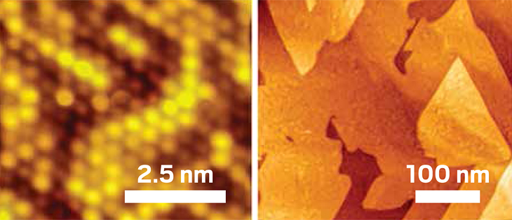
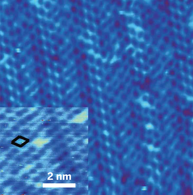
These scanning tunneling microscope images show a single layer of tin, or stanene (atomic resolution image, left), which was grown via a deposition method known as molecular beam epitaxy.
Germanene
Ge
Description: A buckled sheet of germanium atoms arranged in a honeycomb pattern.
Properties & potential applications: Predicted to exhibit high charge-carrier mobility and high-temperature superconductivity, 2-D germanene may eventually find use in electronics and optical devices.
Key citation: New J. Phys. 2014, DOI: 10.1088/1367-2630/16/9/095002
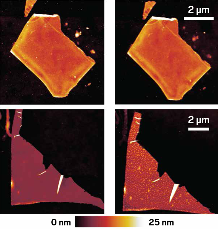
This atomically thin germanene film measures 16.2 nm x 16.2 nm (close-up shown in inset). It was grown via a deposition method called molecular beam epitaxy on a gold surface and then mechanically exfoliated.
Phosphorene
P
Description: A buckled sheet of phosphorus atoms arranged in a honeycomb pattern.
Properties & potential applications: Scientists can isolate phosphorene by separating black phosphorus into atomic layers. The material exhibits a tunable band gap and conducts positive charge. Those properties may make the semiconductor useful for fast flexible electronics and energy storage.
Key citations:
ACS Nano 2014, DOI: 10.1021/nn501226z
Nat. Chem. 2016, DOI: 10.1038/nchem.2505
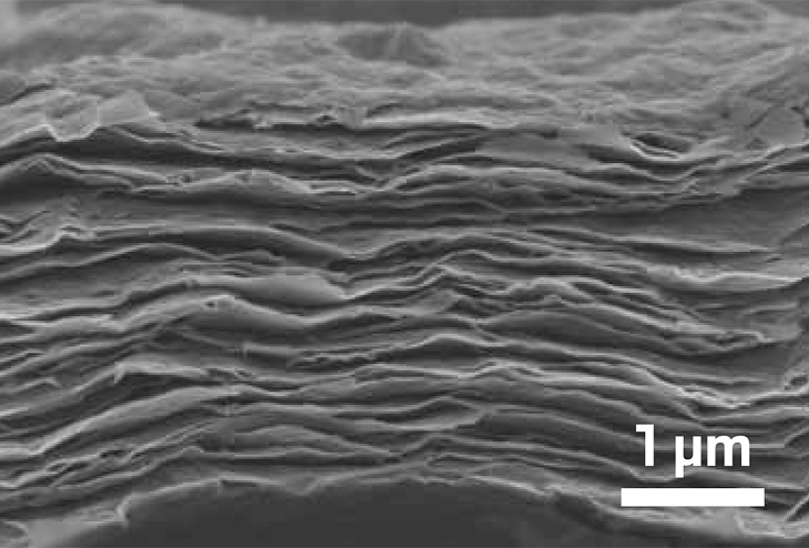
A flake of black phosphorus treated with a benzenediazonium derivative shows no sign of change even after being exposed to air for 10 days (top row). An untreated flake roughens and develops protrusions (light-colored spots) as a result of oxidation (bottom row), as seen in these AFM images.
Transition metal dichalcogenides
MoS2, WS2, and others
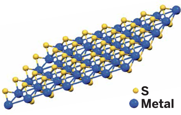
Description: Semiconductor sheets in which a transition metal atom is sandwiched between two chalcogenide atoms.
Properties & potential applications: Because of their pronounced bandgaps, MoS2, WS2, ReS2 and other members of this group have been used to fabricate transistors and other circuit elements for lightweight, flexible electronics.
Key citation: MRS Bull. 2015, DOI: 10.1557/mrs.2015.121
MoS2 and WS2 can now be grown as atomically thin films with a measured area of 10 sq in.
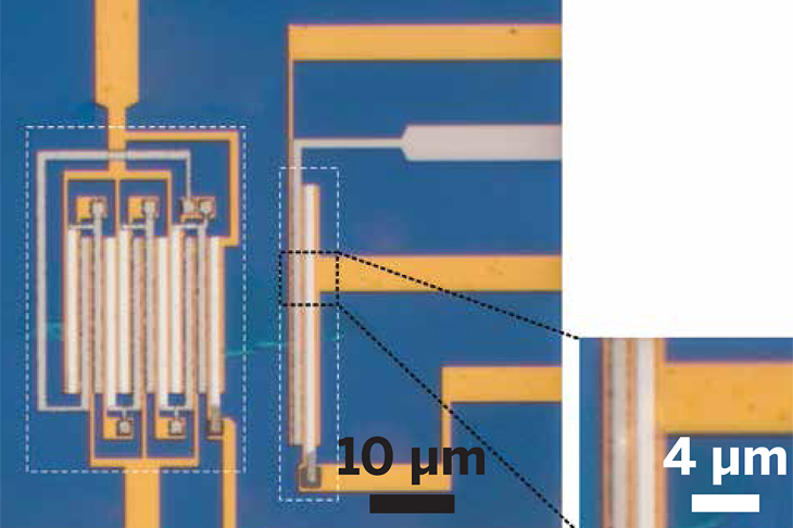
A molecularly thin film of MoS2 serves as the material on which the complex integrated logic circuits seen in this optical micrograph have been fabricated. The device outlined on the left is a five-stage ring oscillator. Next to it is an inverter.
Organic Materials
C
Description: Various crystalline organic compounds composed of stacked molecular sheets; examples include covalent organic frameworks and 2-D polymers.
Properties & potential applications: The properties of these materials are widely tunable via organic chemistry. Some of these materials are highly conjugated and porous, making them promising candidates for nanoporous filters and membranes, biosensors, and optoelectronic devices.
Key citations:
Macromol. Chem. Phys. 2016, DOI: 10.1002/macp.201500312
Adv. Mater. 2015, DOI: 10.1002/adma.201500124
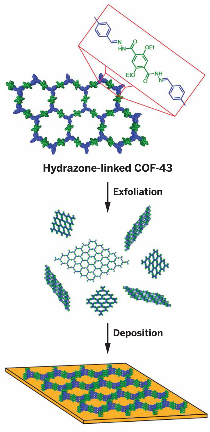
Dioxane and other common solvents can exfoliate hydrazone-linked covalent organic frameworks (COFs). This simple method can be used to prepare and deposit ultrathin COF samples for analysis and applications.
Gallium Nitride
GaN
Description: Formed by allowing nitrogen atoms to diffuse under a protective layer of graphene where they react with trapped gallium atoms.
Properties & potential applications: Two-dimensional GaN's band gap is larger than its bulk counterpart, making this material attractive for electronic and optoelectronic applications.
Key citation: Nat. Mater. 2016, DOI: 10.1038/nmat4742
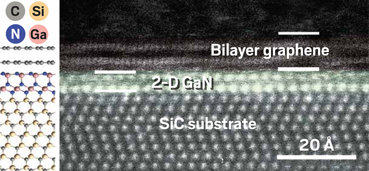
Gallium and nitrogen atoms entrench between a silicon carbide substrate and graphene to form 2-D GaN, as seen in this schematic and electron micrograph.
Boron Nitride
BN
Description: A layered material with a hexagonal honeycomb structure of alternating boron and nitrogen atoms.
Properties & potential applications: BN has been made via vapor deposition and exfoliation. In ultrathin films, BN retains a large band gap and dielectric properties. It could serve as an insulator for high-speed, transparent, flexible electronics.
Key citation: Semicond. Semimetals 2016, DOI: 10.1016/bs.semsem.2016.04.004
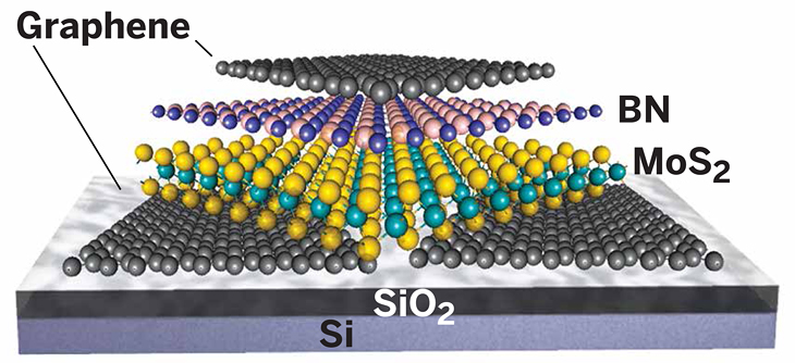
Built on a silicon wafer, an ultrathin transistor made with 2-D materials uses graphene for electrodes, molybdenum disulfide as its semiconductor layer, and boron nitride as an insulator.
Calcium Nitride
Ca2N
Description: A layered ionic solid known as an electride, featuring planes of atoms separated by sheets of delocalized electrons.
Properties & potential applications: Due to the high electrical conductivity of ultrathin sheets of electrides, researchers are developing these materials for battery applications.
Key citation: J. Am. Chem. Soc. 2016, DOI: 10.1021/jacs.6b10114
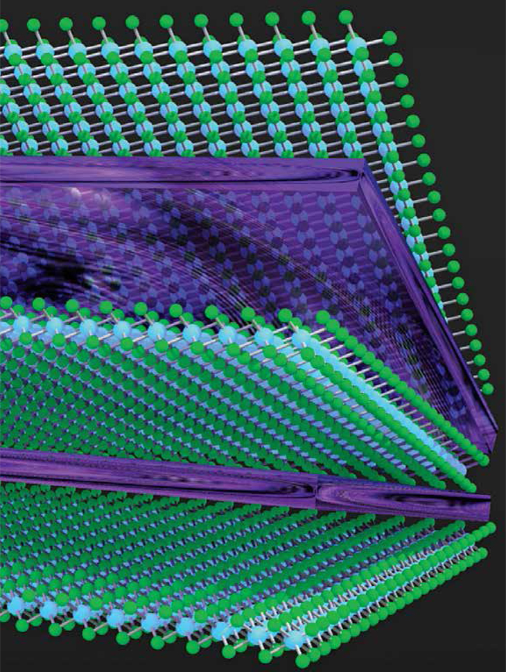
Ca2N, an electride, consists of layers of calcium and nitrogen atoms (green and blue) separated by layers of electrons (purple).