Advertisement
Grab your lab coat. Let's get started
Welcome!
Welcome!
Create an account below to get 6 C&EN articles per month, receive newsletters and more - all free.
It seems this is your first time logging in online. Please enter the following information to continue.
As an ACS member you automatically get access to this site. All we need is few more details to create your reading experience.
Not you? Sign in with a different account.
Not you? Sign in with a different account.
ERROR 1
ERROR 1
ERROR 2
ERROR 2
ERROR 2
ERROR 2
ERROR 2
Password and Confirm password must match.
If you have an ACS member number, please enter it here so we can link this account to your membership. (optional)
ERROR 2
ACS values your privacy. By submitting your information, you are gaining access to C&EN and subscribing to our weekly newsletter. We use the information you provide to make your reading experience better, and we will never sell your data to third party members.
2-D Materials
Researchers grow thin 2-D insulator on large scale
Single-crystal boron nitride could enable the use of 2-D materials for transistors in computer chips
by Neil Savage, special to C&EN
March 4, 2020

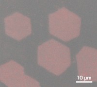
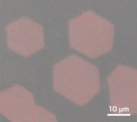
In their unending quest to cram as many circuits onto a computer chip as possible, chipmakers are experimenting with making components from 2-D materials just a few atoms thick. But while they can produce 2-D semiconductors on useful scales, making other materials, such as 2-D insulators, on a large scale has been difficult. Now researchers have found that they can make large single crystals of boron nitride that should fit with the chip-building process (Nature 2020, DOI: 10.1038/s41586-020-2009-2).
Chip researchers have been experimenting with 2-D semiconductors, such as molybdenum disulfide or tungsten disulfide, which are no thicker than the number of atoms needed to make the particular molecule. These materials’ higher electron mobility could make them superior to silicon used in current transistors. To make super-small transistors with these semiconductors, chipmakers would also need a thin insulator. A single layer of the 2-D material hexagonal boron nitride is the thinnest known, and also perfectly flat and chemically inert. Researchers have been looking for a cost-effective way to make single-crystal monolayers of boron nitride 300 mm across to fit the standard wafer size used in chipmaking.
One way to grow crystals of boron nitride is a method called chemical vapor deposition, in which volatile precursors of the material deposit onto a surface in a vacuum chamber. The trouble is that when the boron nitride lands on a copper surface, the flakes that initially form have different spatial orientations. The flakes act as nucleation sites, and as a crystal grows from one, it eventually meets a crystal growing from another flake with a different orientation. When the crystals meet, they form a grain boundary, with a boron atom next to a boron atom or a nitrogen next to a nitrogen, instead of boron next to nitrogen. “You get a bad quality crystal,” says Boris Yakobson of Rice University, who helped develop the new method with chipmaker Taiwan Semiconductor Manufacturing Corporation (TSMC) and academic colleagues in China and Taiwan. Grain boundaries in the insulator can scatter electrons and reduce the quality of transistors.
The trick to avoiding those boundaries turns out to be as simple as controlling the substrate the crystal is grown on. The team started with a layer of sapphire on which they deposited a thin film of copper. The copper tends to form twin grains, with one pointing in one direction and its twin pointing in the opposite. When the team annealed the copper at 1,050 °C, however, the twin grains disappeared.
Yakobson says that even though the copper is essentially flat, at the atomic level there are small steps, and the boron nitride prefers to nucleate along these steps. By using annealing to control the orientation of the copper atoms, the researchers made the steps line up and encouraged the boron nitride crystal to grow in just one direction.
Researchers can peel off the resulting monocrystalline boron nitride from the copper and then place it on another surface. The team grew a 5-cm crystal and placed it on a field-effect transistor made of MoS2. The device had better electron mobility than similar devices made with polycrystalline boron nitride.
Lain-Jong Li, director of corporate research at TSMC, says the MoS2 was used for a proof-of-principle test, but the boron nitride should work as well with other 2-D semiconductors, and no one has decided what future transistors will be made of. The method should alsoscale up to 300 mm, he says. There is not yet a timeline for when 2-D-material-based chips would be commercially available.
“This is a suitable means to grow wafer-scale single-crystal hexagonal boron nitride,” says Ki Kang Kim of the Nanomaterials Synthesis Research Laboratory at Sungkyunkwan University. The growth method might not be compatible with 2-D materials that contain sulfur, he says, because copper and sulfur tend to react.


Join the conversation
Contact the reporter
Submit a Letter to the Editor for publication
Engage with us on Twitter