Advertisement
Grab your lab coat. Let's get started
Welcome!
Welcome!
Create an account below to get 6 C&EN articles per month, receive newsletters and more - all free.
It seems this is your first time logging in online. Please enter the following information to continue.
As an ACS member you automatically get access to this site. All we need is few more details to create your reading experience.
Not you? Sign in with a different account.
Not you? Sign in with a different account.
ERROR 1
ERROR 1
ERROR 2
ERROR 2
ERROR 2
ERROR 2
ERROR 2
Password and Confirm password must match.
If you have an ACS member number, please enter it here so we can link this account to your membership. (optional)
ERROR 2
ACS values your privacy. By submitting your information, you are gaining access to C&EN and subscribing to our weekly newsletter. We use the information you provide to make your reading experience better, and we will never sell your data to third party members.
Synthesis
Atomic-scale Manipulation
by Susan R. Morrissey
September 20, 2004
| A version of this story appeared in
Volume 82, Issue 38

NANOTECH RESEARCH
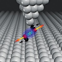
Researchers at the National Institute of Standards & Technology have taken one step closer to making real atomic-scale devices. Joseph A. Stroscio and Robert J. Celotta, both physicists at NIST, used a scanning tunneling microscope to drag a cobalt atom over a copper surface and found that they were able to distinguish between two different crystal-packed binding sites [Science, published online Sept. 9, http://www.sciencemag.org/cgi/content/abstract/1102370v1].
According to Stroscio, this experiment is a new form of measurement, which he calls "atom-based metrology," where the Co atom is serving as a transducer to measure the local properties of a surface. In this work, the Co atom transducer was observed switching from one binding site to another, which told the researchers how to control and improve atom manipulation.
"The main impact of this work is that we better understand the atom manipulation process so we can make it more reliable and extend it more easily to other systems, such as placing atoms on semiconductor substrates to make real nanoscale devices," Stroscio tells C&EN.


Join the conversation
Contact the reporter
Submit a Letter to the Editor for publication
Engage with us on Twitter