Advertisement
Grab your lab coat. Let's get started
Welcome!
Welcome!
Create an account below to get 6 C&EN articles per month, receive newsletters and more - all free.
It seems this is your first time logging in online. Please enter the following information to continue.
As an ACS member you automatically get access to this site. All we need is few more details to create your reading experience.
Not you? Sign in with a different account.
Not you? Sign in with a different account.
ERROR 1
ERROR 1
ERROR 2
ERROR 2
ERROR 2
ERROR 2
ERROR 2
Password and Confirm password must match.
If you have an ACS member number, please enter it here so we can link this account to your membership. (optional)
ERROR 2
ACS values your privacy. By submitting your information, you are gaining access to C&EN and subscribing to our weekly newsletter. We use the information you provide to make your reading experience better, and we will never sell your data to third party members.
Materials
Laser Method Yields Single-Atom-Thick Molybdenum Disulfide
Nanomaterials: Simple technique could lead to MoS2-based electronics
by Prachi Patel
June 8, 2012

Graphene promises electronic circuits that are smaller, faster, and more flexible than those made with silicon. But it’s not the only material that could replace silicon. Researchers have also proposed single-atom-thick layers of molybdenum disulfide, because they have a key electronic property that graphene lacks. With hopes of enabling large-scale production of devices, researchers have now found a simple technique for making one-atom-thick MoS2 (Nano Lett., DOI: 10.1021/nl301164v).
Electrons move through graphene 100 times faster than in silicon, leading to faster-switching transistors, the building blocks for computer logic circuits. Unlike silicon, though, graphene lacks a band gap, the energy needed to move an electron between a conducting state and a nonconducting one. “Because it has no band gap, you can never turn a transistor completely off,” says Andres Castellanos-Gomez, a researcher at Delft University of Technology, in the Netherlands.
Meanwhile, single-atom-thick MoS2 has a band gap larger than silicon’s, which means transistors made from the material not only turn off but require less power to do so. And while MoS2 does not conduct electrons as quickly as graphene, it is strong, flexible, and transparent, just as graphene is.
Currently, no quick, easy way exists to make single-atom sheets of MoS2. Researchers typically exfoliate single layers from a chunk of the material using sticky tape, or they peel layers apart in a chemical solvent. These cumbersome processes mean researchers can make only a few devices at a time.
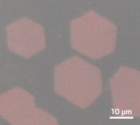
Castellanos-Gomez chanced upon a simple MoS2 thinning technique while he was studying the material’s electronic properties. When he shined a 10-mW green laser beam on multilayer MoS2 flakes, the material’s top layers vaporized. He, his postdoctoral advisor Gary Steele, and their colleagues used optical microscopy, atomic force microscopy, and Raman spectroscopy to confirm that the remaining material, at 1 nm thick, was a single layer of atoms. They also produced transistors using the material and found the devices had switching speeds similar to those of transistors made from exfoliated single-layer flakes.
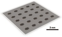
The laser scanning method can make single-layer MoS2 in practically any pattern and size, Castellanos-Gomez says, which could allow the researchers to create complex circuits with dozens of transistors. By carefully tweaking the laser power, he adds, he and his team can thin the material to different extents, creating, for instance, three- or five-atom-thick layers. MoS2 films of different thicknesses show unique properties for applications such as gas-sensing and light-emission. If they combined regions of different thicknesses in a single circuit, the researchers say they could fashion sensors and optoelectronic devices.
The laser thinning method provides a simple route to single-layer MoS2, “which is impossible with the current methods,” says Hua Zhang, who studies two-dimensional nanomaterials at Nanyang Technological University, in Singapore. Its simplicity will allow for applications of single-layer MoS2, he says. But he points out that to make the method feasible for large-scale production, the researchers will have to reduce the time it takes the laser to vaporize the MoS2 layers.


Join the conversation
Contact the reporter
Submit a Letter to the Editor for publication
Engage with us on Twitter