Advertisement
Grab your lab coat. Let's get started
Welcome!
Welcome!
Create an account below to get 6 C&EN articles per month, receive newsletters and more - all free.
It seems this is your first time logging in online. Please enter the following information to continue.
As an ACS member you automatically get access to this site. All we need is few more details to create your reading experience.
Not you? Sign in with a different account.
Not you? Sign in with a different account.
ERROR 1
ERROR 1
ERROR 2
ERROR 2
ERROR 2
ERROR 2
ERROR 2
Password and Confirm password must match.
If you have an ACS member number, please enter it here so we can link this account to your membership. (optional)
ERROR 2
ACS values your privacy. By submitting your information, you are gaining access to C&EN and subscribing to our weekly newsletter. We use the information you provide to make your reading experience better, and we will never sell your data to third party members.
Materials
A Home For Cobalt In Computer Chips
The element is the latest to be integrated into the semiconductor manufacturing process
by Michael McCoy
August 25, 2014
| A version of this story appeared in
Volume 92, Issue 34

Hafnium. Ruthenium. Tantalum. Zirconium. Now cobalt can be added to that list.
As the semiconductor industry tries to uphold Moore’s law—Gordon Moore’s 1965 prediction that the number of transistors in a computer chip will double every two years—silicon is no longer its only significant chip-making material. These days the industry is reaching deep into the periodic table for the ingredients needed to fabricate its most advanced chips.
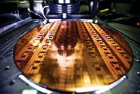
Cobalt is the latest element to be tapped. Applied Materials, a major manufacturer of chip fabrication equipment, is working with its electronics industry customers to incorporate thin cobalt films into semiconductor architecture. And behind the scenes, several chemical companies are jockeying to supply the organometallic precursors needed to make cobalt happen.
Like hafnium oxide in transistors and tantalum nitride in barrier layers, cobalt is being added to the chip fabrication regimen to make the devices work at increasingly tiny dimensions.
In the semiconductor industry’s early days, circuit lines were made on a silicon wafer by etching trenches into a layer of silicon dioxide and filling them with aluminum metal. But as line widths shrank, aluminum’s shortcomings as a conductor became apparent. In 1997, IBM pioneered the switch away from aluminum to copper interconnects.
It wasn’t an easy swap. A dielectric material that insulates better than silicon dioxide was needed. Then, a thin barrier layer of tantalum nitride plus a liner of tantalum had to be applied to the trenches to keep the copper from diffusing into the dielectric.
And to apply copper to the wafer, materials scientists had to develop a new electrodeposition technique because the etching process used with aluminum didn’t work. The new method had two steps: deposition of a thin seed layer of copper to make sure the trench walls were completely covered and then a more complete copper electrodeposition.
With those modifications in place, copper faithfully did its job for many years. At the time it was introduced, circuit lines were 220 nm wide. But today, as circuitry has shrunk to widths of 22 nm and below, new problems are emerging for copper.
A big one, explains David Thompson, Applied Materials’ technology director for process chemistries, is electromigration. Running electric current—electrons—through the ultrathin wires can dislocate copper ions, creating voids in the circuit and opening the door to chip failure.
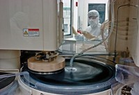
Applied Materials says it has ensured copper’s role for several more chip generations by adapting its Endura Volta deposition equipment to apply a less than 20-Å film of cobalt metal, instead of the tantalum liner, via chemical vapor deposition (CVD) of an organocobalt precursor. The company calls the introduction of cobalt “the most significant materials change to the interconnect in over 15 years.”
Cobalt, the firm’s chemists found, provides better “wetting” of copper than tantalum does. As a result, copper adheres better to the sides of the trenches, minimizing later electromigration.
Thompson is particularly proud of part two of his firm’s cobalt system: a cobalt cap that is deposited selectively over the copper circuit lines, effectively encasing them in a sleeve of cobalt. That step, the company says, represents the first commercially significant use of selective metal chemistry in semiconductor manufacturing.
Why cobalt and not some other material? “The comical answer,” Thompson says, “is ‘because it works.’ ” Elements such as manganese and ruthenium were tested, but cobalt prevailed when it came to low interaction with other materials and robustness in the face of subsequent chip cleaning, polishing, and etching steps.
Although Applied Materials publicly revealed the cobalt system in May, the company says it has been working with the metal for close to a decade. To date, the firm has shipped more than 75 cobalt CVD chambers for use in high-volume manufacturing of chips with sub-22-nm circuitry.
Thompson won’t disclose much about the cobalt precursors used other than to say different chemistries are used for the liner and cap steps. Information about the firms that Applied Materials qualified to supply the chemicals is also proprietary, he says.
But cobalt is definitely a big deal for materials suppliers, confirms Mike Corbett, an analyst with the electronics materials advisory firm Linx Consulting. “This is really the first new element to be integrated into the interconnect in a long while,” he says.
Business opportunity exists both for organometallic chemical specialists, such as Sigma-Aldrich and Digital Specialty Chemicals (DSC), and for industrial gas companies such as Air Liquide and Air Products & Chemicals.
The gases firms traditionally set up facilities inside semiconductor plants that supply both their own gases and chemicals mostly made by other companies. Supply lines are starting to blur, however.
Air Products has been investing in thin-film material capabilities. And last year, Air Liquide acquired Voltaix, a New Jersey-based company that brought high-volume precursor manufacturing capacity.

Given that Applied Materials is targeting cobalt at chips with circuitry of less than 22 nm, the semiconductor giant Intel is probably the only firm currently using it in large volumes, Corbett figures. But companies such as Taiwan Semiconductor Manufacturing Co., which makes chips for third parties under contract, are likely close behind.
The market is already growing. In response to demand from the semiconductor industry, Toronto-based DSC has scaled up production of organocobalt precursors. DSC declines to be more specific about its cobalt line, but a company newsletter indicates that it is manufacturing at least two precursors: cyclopentadienylcobalt dicarbonyl and dicobalt hexacarbonyl tert-butylacetylene.
Manufacturing organometallic precursors isn’t for the faint of heart, cautions Ravi K. Laxman, DSC’s vice president for electronics. Cobalt-containing compounds, for example, tend to be light sensitive, so reactions at DSC’s plant in Toronto have to be carried out in complete darkness.
“If you are making 5 or 10 g at the bench scale, you can just turn off the lights and put a shield around it,” he says. “But when you start manufacturing 10, 50, or 100 kg, it becomes a little challenging to do in the dark.”
DSC also sees an opportunity to help customers deposit tantalum nitride using pentakis(dimethylamino) tantalum (PDMAT), a precursor the firm is now producing at commercial scale. Tantalum nitride is usually applied via physical vapor deposition (PVD) of tantalum metal, but at the tight geometries of sub-22-nm chips, PVD can cause bulges in the circuit trench that inhibit subsequent deposition of copper.
PDMAT, in contrast, can be applied with atomic layer deposition (ALD), a CVD method that deposits smooth films one atomic layer at a time. On its own or with cobalt, ALD-applied tantalum nitride can reduce electromigration and help preserve copper’s low resistivity, according to Laxman.
But synthesizing PDMAT, a solid at room temperature, presents its own challenges, Laxman says. Trace amounts of oxygen can cause tantalum to behave like a capacitor rather than a barrier, so DSC developed a series of purification steps to yield a PDMAT that is more than 99.99995% pure.
Laxman notes that chip fabrication plants are not necessarily making a choice between cobalt and tantalum. “As you go below 22 nm, every fab is adapting different materials,” he says. Some firms may even decide to use a cobalt precursor on some circuitry levels and PDMAT on others. “We see a tremendous amount of growth happening for all of them,” Laxman adds.
Indeed, Linx’s Corbett estimates that the cobalt precursors business is already worth tens of millions of dollars per year. As more chip makers adopt cobalt as a companion to copper, volumes will rise, although prices will also come down. On balance, Corbett expects that the market “could be a $75 million opportunity.”
At the same time, semiconductor engineers who become comfortable with cobalt will start to explore the metal for other applications in the chip-making process. “We expect to see more and more cobalt ALD and CVD going forward,” Corbett says.
If and when that happens, Applied Materials is sure to be enlisting its chemical industry partners again. “It’s not always easy to guess which materials are going to be the winners and which are the losers,” Thompson says. “We have to be in lockstep with our chemical suppliers so they are able to scale up in a timely fashion.”


Join the conversation
Contact the reporter
Submit a Letter to the Editor for publication
Engage with us on Twitter