Advertisement
Grab your lab coat. Let's get started
Welcome!
Welcome!
Create an account below to get 6 C&EN articles per month, receive newsletters and more - all free.
It seems this is your first time logging in online. Please enter the following information to continue.
As an ACS member you automatically get access to this site. All we need is few more details to create your reading experience.
Not you? Sign in with a different account.
Not you? Sign in with a different account.
ERROR 1
ERROR 1
ERROR 2
ERROR 2
ERROR 2
ERROR 2
ERROR 2
Password and Confirm password must match.
If you have an ACS member number, please enter it here so we can link this account to your membership. (optional)
ERROR 2
ACS values your privacy. By submitting your information, you are gaining access to C&EN and subscribing to our weekly newsletter. We use the information you provide to make your reading experience better, and we will never sell your data to third party members.
Materials
Liquid metals yield large 2-D semiconductor films
Spontaneously forming oxide skin offers route to converting gallium, other metals to sulfides
by Mitch Jacoby
February 27, 2017
| A version of this story appeared in
Volume 95, Issue 9

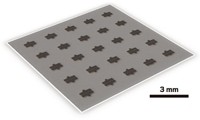
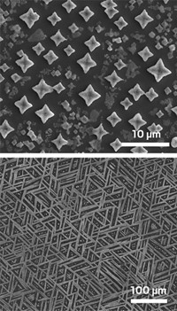
The curious properties of gallium and related liquid metals, “especially the tendency to spontaneously form thin oxide skins in air,” have led researchers in recent years to use these materials for chemical patterning and for making stretchy and self-healing electronics. Now, a team of researchers in Australia and the U.S. has exploited that property to prepare these materials as large, ultrathin patterned semiconductor films via methods that are compatible with electronics industry manufacturing (Nat. Commun. 2017, DOI: 10.1038/ncomms14482). Due to their potential use in microelectronic devices, metal sulfides and other semiconducting chalcogenide compounds keep grabbing attention—especially when researchers report methods for preparing them as atomically thin films. But many of those methods require high temperatures or yield tiny defective flakes, rendering the methods incompatible with the semiconductor industry. Torben Daeneke and Kourosh Kalantar-Zadeh of RMIT University, Melbourne, and coworkers show that those problems can be avoided by using liquid metals. The team deposited gallium on a wafer-sized substrate that had been patterned with a fluorinated compound and then converted the gallium oxide to a high-quality 1.5-nm-thick film of gallium sulfide. The team used a similar method to make large In2S3 films and showed that the materials can be used to build transistors.


Join the conversation
Contact the reporter
Submit a Letter to the Editor for publication
Engage with us on Twitter