Advertisement
Grab your lab coat. Let's get started
Welcome!
Welcome!
Create an account below to get 6 C&EN articles per month, receive newsletters and more - all free.
It seems this is your first time logging in online. Please enter the following information to continue.
As an ACS member you automatically get access to this site. All we need is few more details to create your reading experience.
Not you? Sign in with a different account.
Not you? Sign in with a different account.
ERROR 1
ERROR 1
ERROR 2
ERROR 2
ERROR 2
ERROR 2
ERROR 2
Password and Confirm password must match.
If you have an ACS member number, please enter it here so we can link this account to your membership. (optional)
ERROR 2
ACS values your privacy. By submitting your information, you are gaining access to C&EN and subscribing to our weekly newsletter. We use the information you provide to make your reading experience better, and we will never sell your data to third party members.
2-D Materials
Scientists synthesize large borophene crystals
A new method could help researchers bring the material closer to applications
by Sam Lemonick
November 4, 2021
| A version of this story appeared in
Volume 99, Issue 41

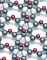
Scientists have stumbled on a new way to make borophene that lets them make large sheets of the 2D material and protect it from degradation (Sci. Adv. 2021, DOI: 10.1126/sciadv.abk1490). While exploring chemical vapor deposition (CVD)—in which a vapor condenses on a surface to make a 2D material—using borazine (B3H6N3) to make boron nitride in its hexagonal crystal form (hBN), researchers discovered their B3H6N3 supply was contaminated with diborane. Marc González Cuxart and Willi Auwärter of the Technical University of Munich and Hermann Sachdev, most recently of Bundeswehr University Munich, realized that CVD of diborane would make borophene.
Calculations have shown that borophene, which was first synthesized in 2015, should have properties comparable to graphene that could make it useful in batteries and other devices. But researchers have been able to make crystals only tens of nanometers wide. The researchers were able to use CVD to make sheets of borophene about 1 µm wide.
“The demonstration of large single-crystalline domains is an important step towards realizing the potential of borophene,” Mark Hersam of Northwestern University says. He was part of one of the first groups to make borophene. The study authors say producing larger amounts of borophene for potential applications is one advantage of the method and add that larger crystals will also enable others to test some of the material’s predicted properties.
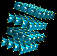
In addition to making borophene, the CVD technique lets the team make layers of hBN. Because boron reacts readily with a number of elements, borophene can quickly degrade when exposed to air. But hBN is much more inert. The researchers developed a system to deposit borophene on iridium and copper surfaces, followed by a layer of hBN. The hBN protected the borophene from oxidation in tests with molecular oxygen.
One limitation of the method is that it requires deposition in a very clean environment, so the researchers performed their syntheses at less than about 100 nPa of pressure.


Join the conversation
Contact the reporter
Submit a Letter to the Editor for publication
Engage with us on Twitter