Advertisement
Grab your lab coat. Let's get started
Welcome!
Welcome!
Create an account below to get 6 C&EN articles per month, receive newsletters and more - all free.
It seems this is your first time logging in online. Please enter the following information to continue.
As an ACS member you automatically get access to this site. All we need is few more details to create your reading experience.
Not you? Sign in with a different account.
Not you? Sign in with a different account.
ERROR 1
ERROR 1
ERROR 2
ERROR 2
ERROR 2
ERROR 2
ERROR 2
Password and Confirm password must match.
If you have an ACS member number, please enter it here so we can link this account to your membership. (optional)
ERROR 2
ACS values your privacy. By submitting your information, you are gaining access to C&EN and subscribing to our weekly newsletter. We use the information you provide to make your reading experience better, and we will never sell your data to third party members.
Surface Chemistry
Rudy Wojtecki
Nanopatterning virtuoso is building the electronics of the future
by Mitch Jacoby
August 14, 2020
| A version of this story appeared in
Volume 98, Issue 31

Credit: Courtesy of Rudy Wojtecki (Wojtecki); Rudy Wojtecki/IBM (illustration); ACS Appl. Mater. Interfaces (micrograph); Shutterstock (circuit)
If Rudy Wojtecki had to pick just one area of science to excel in, he’d be stuck. His coworkers say he does a bang-up job in a whole bunch of areas, not just patterning nanomaterials for tomorrow’s electronics, his main focus. “I’m naturally a curious person,” he says. “I like to understand how all kinds of things work.”
That curiosity has put Wojtecki on a fast track at IBM, where he was hired about 6 years ago to be a technician in the company’s nuclear magnetic resonance (NMR) spectroscopy facility at the Almaden Research Center. But Wojtecki wasn’t content to just maintain NMR instruments, analyze samples, and collect data. So he teamed up with an IBM group studying new materials and often stayed late, doing what he describes as “after-hours research on really interesting polymer systems.” These extracurricular activities soon led to journal publications and patents. It also led higher-ups at IBM, such as Robert D. Allen, senior manager of polymer science and technology, to notice Wojtecki’s multifaceted talent.
Advertisement
In addition to being an NMR expert, Allen says, Wojtecki is also a strong synthetic chemist and polymer chemist, with a broad background in supramolecular chemistry. In the past few years, he has become a specialist in atomic layer deposition (ALD), a surface coating technique for making nanostructured materials and electronic devices. Wojtecki also found time to study quantum computing—now he’s an IBM spokesperson on the subject—and he even invented a new method for decaffeinating coffee.
“Most people do science or technology, but they don’t do both really well,” Allen says. “Rudy just jumps right in, figures out the basic science, and applies it to new technology. He’s a true scientist and technologist.”

The technology Wojtecki focuses on most these days is ALD. He explains that to keep up with demand for ever faster and more powerful computers and mobile devices, manufacturers will need to develop new methods for making the building blocks of electronic circuits. Today’s gadgets rely primarily on lithography for whittling relatively thick semiconductors and carving microscopic circuit features into their surfaces. The methods easily get down to the low nanometer scale. But that’s not small enough for future electronics.
ALD works from the other direction. It deposits one layer of molecules at a time—methodically building up films of insulators and conductors of predetermined thickness. Chipmakers already make limited use of the method, but Wojtecki wants to broaden its reach by developing techniques that control exactly how and where ALD does its thing.
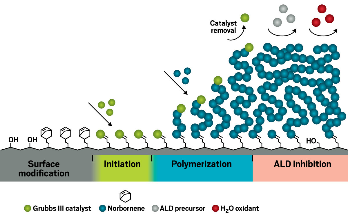
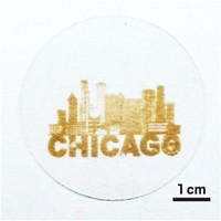
One way he does it is by coating surfaces with extremely thin layers of molecules that bind selectively to some parts of a surface then polymerize on cue. The result is a pattern of defect-free barriers that block ALD films from growing in one spot but not the adjacent spot. That approach, which required Wojtecki to synthesize a host of new reagents with surface-binding ligands and custom polymerization properties, has already yielded patterns with features in the low nanometer size range. And Wojtecki is just getting started.
“The idea that you can take a material from the lab and use it to solve a problem in microelectronics—that really excites me,” he says.
Vitals
Current affiliation: IBM
Age: 35
PhD alma mater: Case Western Reserve University
Hometown: Mantua, Ohio
If I weren’t a chemist, I’d be: A marine scientist specializing in deep-sea creatures. “I have always been fascinated with deep-sea life and how alien it is to the world we know.”
If I were an element, I’d be: Carbon. “This gives rise to such intricate chemical complexity from its bonding. It is a remarkable element.”
If Rudy Wojtecki had to pick just one area of science to excel in, he’d be stuck. His coworkers say he does a bang-up job in a whole bunch of areas, not just patterning nanomaterials for tomorrow’s electronics, his main focus. “I’m naturally a curious person,” he says. “I like to understand how all kinds of things work.”
Vitals
▸ Current affiliation: IBM
▸ Age: 35
▸ PhD alma mater: Case Western Reserve University
▸ Hometown: Mantua, Ohio
▸ If I weren’t a chemist, I’d be: A marine scientist specializing in deep-sea creatures. “I have always been fascinated with deep-sea life and how alien it is to the world we know.”
▸ If I were an element, I’d be: Carbon. “This gives rise to such intricate chemical complexity from its bonding. It is a remarkable element.”
That curiosity has put Wojtecki on a fast track at IBM, where he was hired about 6 years ago to be a technician in the company’s nuclear magnetic resonance (NMR) spectroscopy facility at the Almaden Research Center. But Wojtecki wasn’t content to just maintain NMR instruments, analyze samples, and collect data. So he teamed up with an IBM group studying new materials and often stayed late, doing what he describes as “after-hours research on really interesting polymer systems.” These extracurricular activities soon led to journal publications and patents. It also led higher-ups at IBM, such as Robert D. Allen, senior manager of polymer science and technology, to notice Wojtecki’s multifaceted talent.
In addition to being an NMR expert, Allen says, Wojtecki is also a strong synthetic chemist and polymer chemist, with a broad background in supramolecular chemistry. In the past few years, he has become a specialist in atomic layer deposition (ALD), a surface coating technique for making nanostructured materials and electronic devices. Wojtecki also found time to study quantum computing—now he’s an IBM spokesperson on the subject—and he even invented a new method for decaffeinating coffee.
“Most people do science or technology, but they don’t do both really well,” Allen says. “Rudy just jumps right in, figures out the basic science, and applies it to new technology. He’s a true scientist and technologist.”
The technology Wojtecki focuses on most these days is ALD. He explains that to keep up with demand for ever faster and more powerful computers and mobile devices, manufacturers will need to develop new methods for making the building blocks of electronic circuits. Today’s gadgets rely primarily on lithography for whittling relatively thick semiconductors and carving microscopic circuit features into their surfaces. The methods easily get down to the low nanometer scale. But that’s not small enough for future electronics.
ALD works from the other direction. It deposits one layer of molecules at a time—methodically building up films of insulators and conductors of predetermined thickness. Chipmakers already make limited use of the method, but Wojtecki wants to broaden its reach by developing techniques that control exactly how and where ALD does its thing.
One way he does it is by coating surfaces with extremely thin layers of molecules that bind selectively to some parts of a surface then polymerize on cue. The result is a pattern of defect-free barriers that block ALD films from growing in one spot but not the adjacent spot. That approach, which required Wojtecki to synthesize a host of new reagents with surface-binding ligands and custom polymerization properties, has already yielded patterns with features in the low nanometer size range. And Wojtecki is just getting started.
“The idea that you can take a material from the lab and use it to solve a problem in microelectronics—that really excites me,” he says.


Join the conversation
Contact the reporter
Submit a Letter to the Editor for publication
Engage with us on Twitter